HV441(2001) 查看數據表(PDF) - Supertex Inc
零件编号
产品描述 (功能)
生产厂家
HV441 Datasheet PDF : 7 Pages
| |||
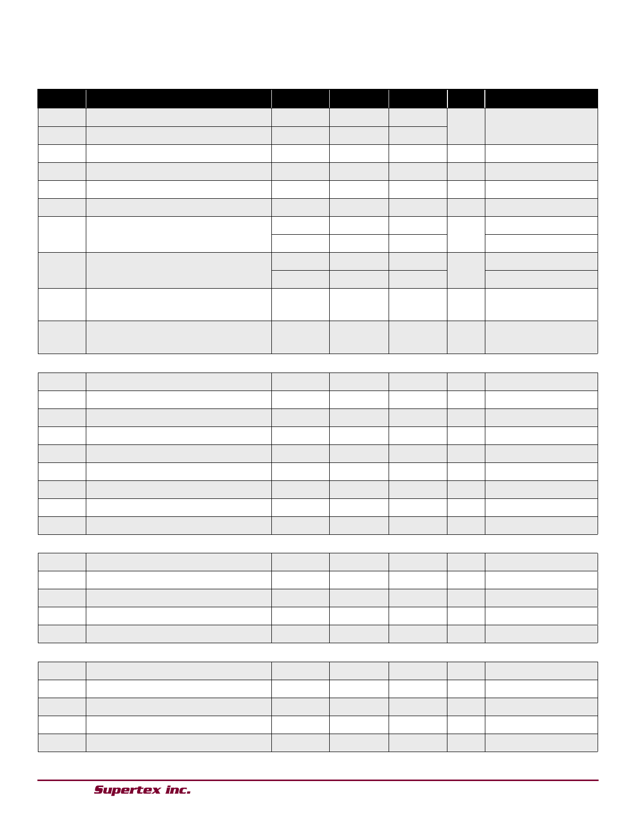
Electrical Characteristics, cont’d.
(Over operating supply voltage unless otherwise specified, TA = 25°C.)
Symbol Parameters
Min
Typ
VPP1
High voltage positive supply
15
VPP2
Positive charge pump output voltage VPP1 – 8
VNN1
High voltage negative supply
VPP – 220
VNN2
Negative charge pump output voltage VNN1 + 5.2
VDD1
Low voltage supply
3.0
VDD2
Low voltage supply
10.8
IPP1Q
VPP1 quiescent current
250
INN1Q
VNN1 quiescent current
250
IPP1
VPP1 operating current
INN1
IDD1Q
IDD2Q
VNN1 operating current
VDD1 quiescent current
VDD2 quiescent current
HV441
Max
110
VPP1 – 19
-110
VNN1 +10.5
5.5
13.5
400
500
0.8
1.0
10
4.0
Unit
V
V
V
V
V
V
µA
µA
mA
mA
Conditions
TA = -40°C to +85°C
TA = -40°C to +85°C
TA = -40°C to +85°C
TA = -40°C to +85°C
TA = -40°C to +85°C
TA = -40°C to +85°C
TA = -40°C to +85°C
TA = -40°C to +85°C
HVOUT switching at 100KHz,
VPP1 = +60V, VNN1 = -160V,
T A = -40°C to +85°C
µA
mA
Pin Description
VPP1
VPP2
VNN1
VNN2
VDD1
VDD2
GND
PGND
Input1-
Input1+
Output1
Input2-
Input2+
Output2
Input3-
Input3+
Output3
Vref
On/Off
osc1
osc2
oscin
oscout
HVOUT
Vpsen
Vnsen
Pgate
Ngate
Positive high voltage supply
Positive gate voltage supply. Generated by an internal linear regulator.
Negative high voltage supply
Negative gate voltage supply. Generated by an internal linear regulator.
+3.3V to 5.0V supply for input and output logic
+12V supply for analog/logic circuit
Low voltage ground
High voltage power ground
Inverting input of op-amp 1.
Noninverting input of op-amp 1.
Output of op-amp 1.
Inverting input of op-amp 2.
Noninverting input of op-amp 2.
Output of op-amp 2.
Inverting input of op-amp 3.
Noninverting input of op-amp 3.
Output of op-amp 3.
External input reference voltage for zero crossing detection.
Enables/Disables HVOUT.
Input 1 for external resonator. Connect to GND when not in use.
Input 2 for external resonator. Leave floating when not in use.
External oscillator input. Zero to VDD1 input signal. Connect to VDD1 when not in use.
Oscillator output; 1/4 frequency of external resonator. 50% duty cycle.
High voltage output. Voltage swings from VPP1 to VNN1.
Pulse by pulse over current sensing for internal P-Channel MOSFET.
Pulse by pulse over current sensing for internal N-Channel MOSFET.
Gate drive for external P-channel MOSFET.
Gate drive for external N-channel MOSFET.
3
Share Link: 