HV6810PJ-G(2013) 查看數據表(PDF) - Supertex Inc
零件编号
产品描述 (功能)
生产厂家
HV6810PJ-G Datasheet PDF : 9 Pages
| |||
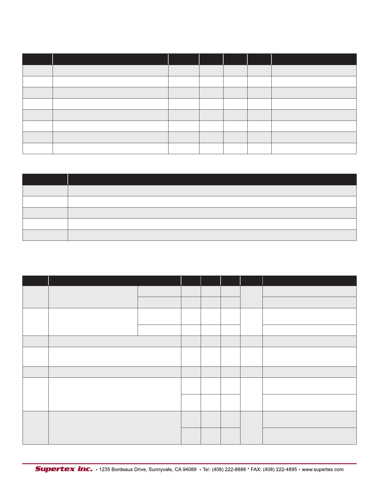
Ordering Information
Part Number
Package Options
Packing
HV6810PJ-G
20-Lead PLCC*
48/Tube
HV6810PJ-G M910 20-Lead PLCC*
1000/Reel
HV6810WG-G
20-Lead SOW
1000/Reel
-G denotes a lead (Pb)-free / RoHS compliant package
* Obsolescence notice issued for the product in the 20-Lead PLCC package.
Pin Configuration
2 1 20
1
HV6810
20
Absolute Maximum Ratings1
Parameter
Value
Logic supply voltage, VDD2
Driver supply voltage, VBB2
Output voltage2
7.5V
90V
90V
Input voltage2
Continuous total power dissipation at
25OC free-air temperature:3
20-Lead PLCC3
20-Lead SOW3
-0.3V to VDD+ 0.3V
1500mW
1500mW
Operating temperature range
-45°C +85°C
Stresses beyond those listed under “Absolute Maximum Ratings” may cause
permanent damage to the device. These are stress ratings only, and functional
operation of the device at these or any other conditions beyond those indicated
in the operational sections of the specifications is not implied. Exposure to
absolute maximum rating conditions for extended periods may affect device
reliability. All voltages are referenced to GND.
Notes:
1. Over operating free-air temperature
2. All voltages are referenced to VSS
3. For operation above 25OC ambient derate linearly to 85OC at 15mW/OC
Typical Thermal Resistance
Package
20-Lead PLCC
θja
66OC/W
20-Lead SOW
66OC/W
20-Lead PLCC
(top view)
20-Lead SOW
(top view)
Product Marking
Top Marking
YY = Year Sealed
YYWW AAA
HV6810PJ
WW = Week Sealed
LLLLLLLLLL L = Lot Number
Bottom Marking
A
C
=
=
Assembler
Country of
ID
Origin*
= “Green” Packaging
CCCCCCCCCCC *May be part of top marking
Package may or may not include the following marks: Si or
20-Lead PLCC
Top Marking YY = Year Sealed
YYWW AAA WW = Week Sealed
HV6810WG
LLLLLLLLLL
A = Assembler ID
L = Lot Number
Bottom Marking C = Country of Origin*
CCCCCCCCCCC
= “Green” Packaging
* May be part of top marking
Package may or may not include the following marks: Si or
20-Lead SOW
Recommended Operating Conditions
Sym Parameter
Min
VDD Supply voltage
4.5
VBB High supply voltage
20
VSS Supply voltage
-
VIH
High-level input voltage (for VDD = 5.0V)
3.5
VIL
Low-level input voltage
-0.3
IOH
Continuous high-level Q output current
25
fCLK
Clock frequency
-
TA
Operating ambient temperature
-40
Doc.# DSFP-HV6810
E070913
2
Typ Max Units Conditions
-
5.5
V ---
-
80
V ---
0
-
V ---
-
5.3
V ---
-
0.8
V ---
-
-
mA ---
-
5.0 MHz ---
-
+85 °C ---
Supertex inc.
www.supertex.com
Share Link: 