HV6810PJ-G 查看數據表(PDF) - Supertex Inc
零件编号
产品描述 (功能)
生产厂家
HV6810PJ-G Datasheet PDF : 8 Pages
| |||
HV6810
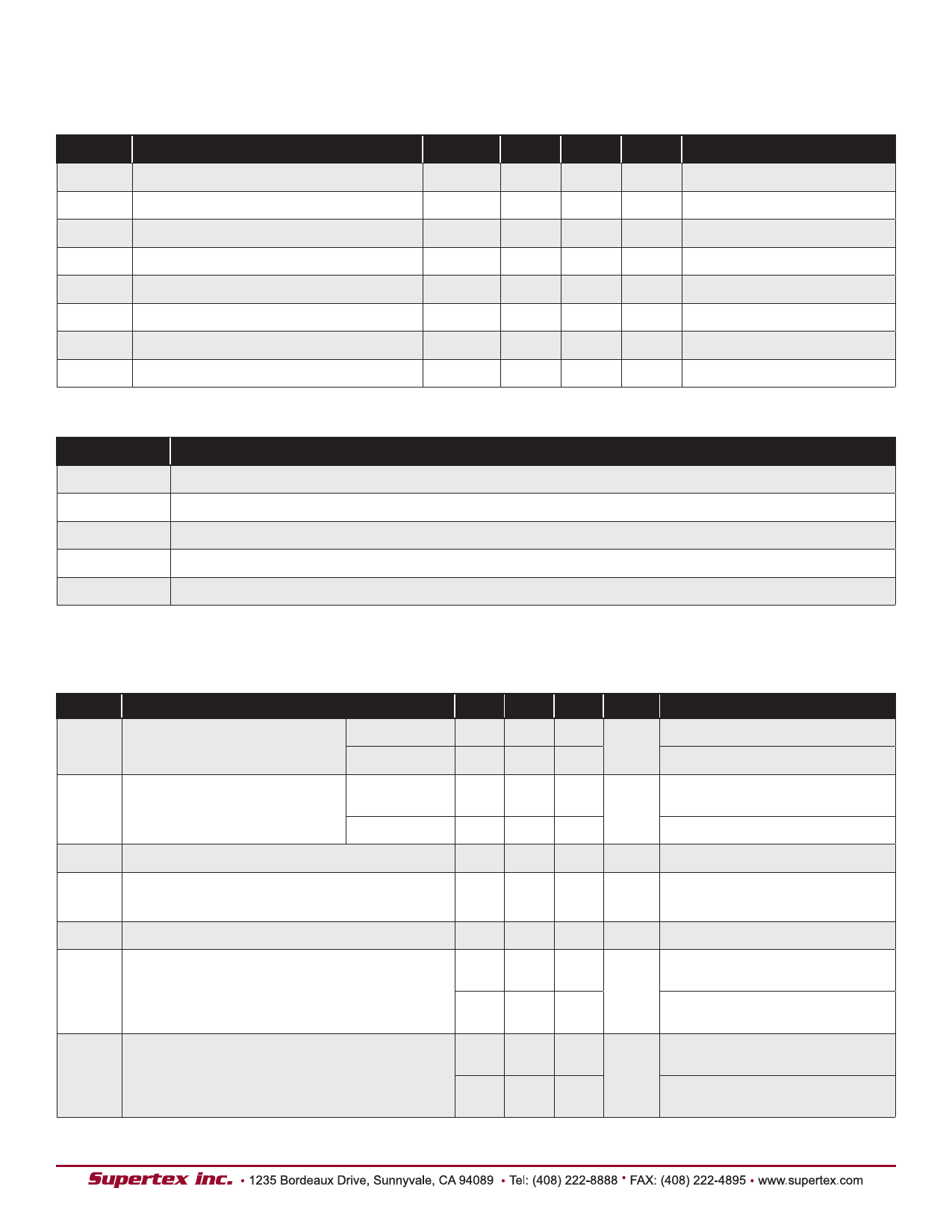
Recommended Operating Conditions
Sym Parameter
Min
VDD Supply voltage
4.5
VBB Supply voltage
20
VSS Supply voltage
-
VIH
High-level input voltage (for VDD = 5.0V)
3.5
VIL
Low-level input voltage
-0.3
IOH
Continuous high-level Q output current
-25
fCLK
Clock frequency
-
TA
Operating ambient temperature
-40
Typ Max Units Conditions
-
5.5
V ---
-
80
V ---
0
-
V ---
-
5.3
V ---
-
0.8
V ---
-
-
mA ---
-
5.0 MHz ---
-
+85 °C ---
Power-Up / Power-Down Sequence
Step
Description
1
Connect ground VSS
2
Apply VDD
3
Set all inputs (Data, CLK, Enable, etc.) to a known state
4
Apply VBB
5
The VBB should not drop below VDD or float during operation.
Power-down sequence should be the reverse of the above.
DC Electrical Characteristics
(VDD = 5V±10%, VBB = 60V, VSS = 0, TA = 25OC unless otherwise noted)
Sym Parameter
VOH High level output voltage
Q outputs
Serial output
VOL Low level output voltage
Q outputs
Serial output
IOL Low level Q output current (pull-down current)
IO(OFF) Off-state output current
IH High level input current
IDD Supply current from VDD (standby)
IBB Supply current from VBB
* All typical values are at TA = 25OC except for IO.
Min
57.5
4.0
-
-
60
-
-
-
-
-
-
Typ
58
4.5
0.15
0.05
80
-1.0
10
10
0.05
0.05
Max
-
-
1.0
0.1
-
-15
1.0
50
50
0.1
0.1
Units
V
V
µA
µA
µA
µA
mA
Conditions
IOH = 25mA
VDD = 4.5V, IOL = -100µA
IOH = 100µA,
blanking input at VDD
VDD = 4.5V, IOL = 100µA
TA = Max, VOL = 0.7V
VO = 0, Blanking input
TA = Max at VDD
Vl = VDD
All inputs at 0V,
one Q output high
All inputs at 0V,
all Q outputs low
All outputs low,
all Q outputs open
All outputs high,
all Q outputs open
2
Share Link: 