HV830LG-G(2013) 查看數據表(PDF) - Supertex Inc
零件编号
产品描述 (功能)
生产厂家
HV830LG-G Datasheet PDF : 6 Pages
| |||
Supertex inc.
HV830
High Voltage EL Lamp Driver IC
Features
►► Processed with HVCMOS® technology
►► 2.0 to 9.5V operating supply voltage
►► DC to AC conversion
►► 200V peak-to-peak typical output voltage
►► Large output load capability typically 50nF
►► Permits the use of high-resistance elastomeric lamp
components
►► Adjustable output lamp frequency to control lamp
color, lamp life, and power consumption
►► Adjustable converter frequency to eliminate harmon-
ics and optimize power consumption
►► Enable/disable function
►► Low current draw under no load condition
►► Very low standby current - 30nA typical
Applications
►► Handheld personal computers
►► Electronic personal organizers
►► GPS units
►► Pagers
►► Cellular phones
►► Portable instrumentation
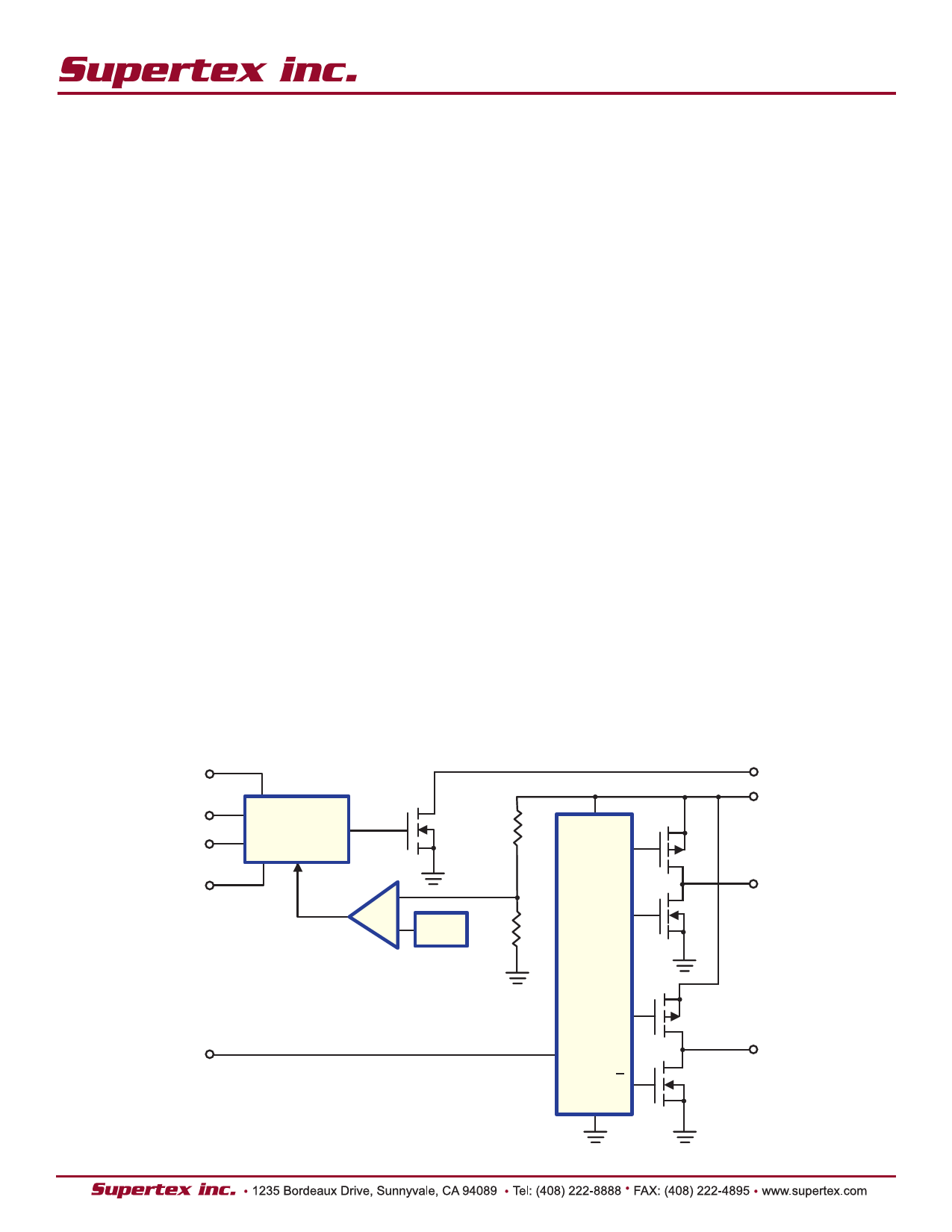
General Description
The Supertex HV830 is a high-voltage driver designed for
driving EL lamps of up to 50nF. EL lamps greater than 50nF
can be driven for applications not requiring high brightness.
The input supply voltage range is from 2.0 to 9.5V. The device
uses a single inductor and a minimum number of passive
components. The nominal regulated output voltage that is
applied to the EL lamp is ±100V. The chip can be enabled
by connecting the resistors on the RSW-Osc and REL-Osc
pins to the VDD pin, and disabled when connected to GND.
The HV830 has two internal oscillators, a switching MOSFET
and a high-voltage EL lamp driver. The frequency of the
switching converter MOSFET is set by an external resistor
connected between the RSW-Osc and the VDD pins. The EL
lamp driver frequency is set by an external resistor connected
between the REL-Osc and the VDD pins. An external induc-
tor is connected between the LX and VDD pins. A 0.01µF to
0.1µF capacitor is connected between the CS pin and the
GND. The EL lamp is connected between the VA and VB pins.
The switching MOSFET charges the external inductor and
discharges it into the CS capacitor. The voltage at CS will
start to increase. Once the voltage at CS reaches a nominal
value of 100V, the switching MOSFET is turned OFF to con-
serve power. The output pins VA and VB are configured as
an H-bridge and are switched in opposite states to achieve
200V peak-to-peak across the EL lamp.
Block Diagram
VDD
RSW-Osc
Switch
Osc
LX
CS
Q
VA
GND
+
Disable
C_
VREF
Q
Output
Osc
REL-Osc
Q
VB
Q
Doc. # DSFP-HV830
E072913
Supertex inc.
www.supertex.com
Share Link: 