HV830(2013) 查看數據表(PDF) - Supertex Inc
零件编号
产品描述 (功能)
生产厂家
HV830 Datasheet PDF : 6 Pages
| |||
HV830
Ordering Information
Part Number
Package
HV830LG-G
8-Lead SOIC
-G denotes a lead (Pb)-free / RoHS compliant package
Packing
2500/Reel
Absolute Maximum Ratings
Parameter
Value
Supply voltage, VDD
Output voltage, VCS
Power dissipation
-0.5 to +10V
-0.5 to +120V
400mW
Storage temperature
-65OC to +150OC
Operating temperature
-25OC to +85OC
Absolute Maximum Ratings are those values beyond which damage to the device may
occur. Functional operation under these conditions is not implied. Continuous operation
of the device at the absolute rating level may affect device reliability. All voltages are
referenced to device ground.
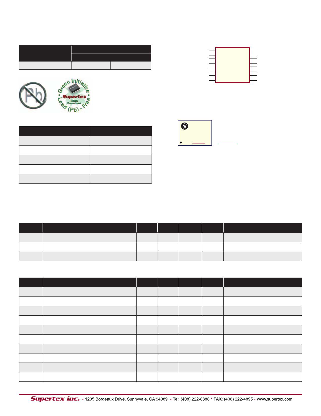
Pin Configuration
VDD 1
8 REL-Osc
RSW-Osc 2
7 VA
CS 3
6 VB
LX 4
5 GND
8-Lead SOIC
(top view)
Product Marking
YWW
HV830
LLLL
Y = Last Digit of Year Sealed
WW = Week Sealed
L = Lot Number
= “Green” Packaging
Package may or may not include the following marks: Si or
8-Lead SOIC
Typical Thermal Resistance
Package
8-Lead SOIC
θja
101OC/W
Recommended Operating Conditions
Sym
VDD
fEL
TA
Parameter
Supply voltage
VA-B output drive frequency
Operating temperature
Min Typ Max Unit Conditions
2.0
-
9.5
V ---
-
-
1.5
KHz ---
-25
-
+85
OC ---
DC Electrical Characteristics (VIN = 3.0V, RSW = 1.0MΩ, REL = 3.3MΩ, TA = 25°C unless otherwise specified)
Sym Parameter
Min Typ Max Unit Conditions
RDS(ON) On resistance of switching transistor
-
2.0
4.0
Ω I = 100mA
VCS Output voltage - regulation
90
100
110
V VDD = 2.0V to 9.5V
VA - VB Output peak-to-peak voltage
180 200
220
V VDD = 2.0V to 9.5V
IDDQ Quiescent VDD current - disabled
-
30
-
nA RSW-Osc = Low
IDD VDD supply current
-
100
150
µA VDD = 3.0V. See Fig.1
IIN Input current including inductor current -
35
40
mA VDD = 3.0V. See Fig.1
VCS Output voltage on VCS
-
95
-
V VDD = 3.0V. See Fig.1
fEL VA - VB output drive frequency
220 250
280
Hz VDD = 3.0V. See Fig.1
fSW Inductor switching frequency
55
65
75
KHz VDD = 3.0V. See Fig.1
D Switching transistor duty cycle
-
88
-
% ---
Doc. # DSFP-HV830
E072913
Supertex inc.
2
www.supertex.com
Share Link: 