HV839MG 查看數據表(PDF) - Supertex Inc
零件编号
产品描述 (功能)
生产厂家
HV839MG Datasheet PDF : 9 Pages
| |||
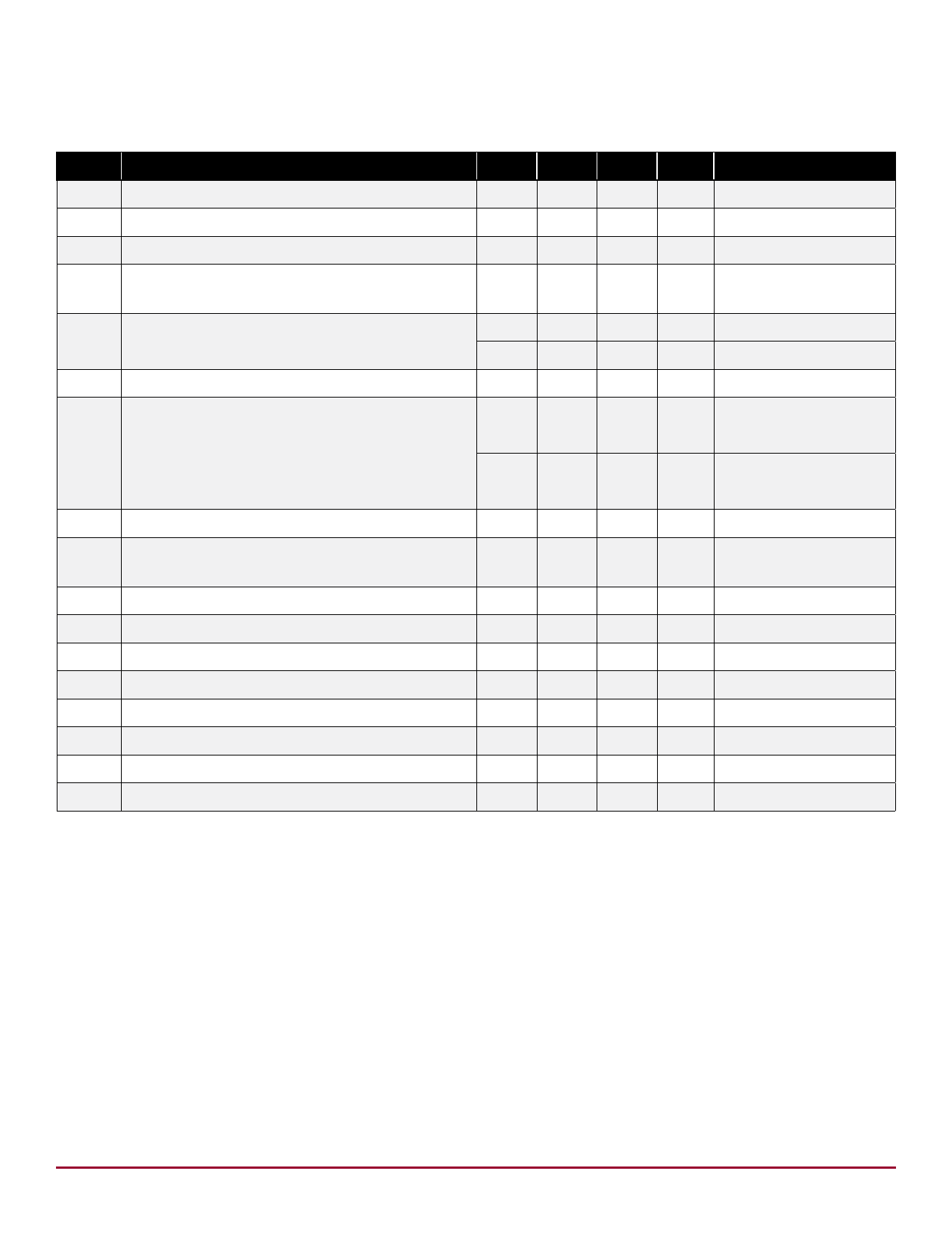
HV839
DC Electrical Characteristics
(Over recommended operating conditions unless otherwise specified. VDD = 2.6 to 5.5V, TA = 25°C)
Sym Parameter
Min Typ Max
RDS(ON)
VDD
VCS
VDIFF
On resistance switching transformer
Input voltage range
Output regulation voltage
Differential peak to peak voltage (EL1 to COM,
EL2 to COM)
-
-
6.0
2.0
-
5.8
80
90 100
160 180 200
IDDQ Quiescent VDD supply current
-
-
150
-
-
500
IDD Input current to the VDD pin
-
-
190
IIN
Input current including inductor current when
driving both lamps
-
-
60
-
45
53
VCS
VDIFF
Output voltage on VCS when driving both lamps
Differential output peak to peak voltage (EL1 to
COM, EL2 to COM)
fEL
fSW
fSW DRIFT
D
VDIF output drive frequency
Switching transistor frequency
Switching transistor frequency drift
Switching transistor duty cycle
IIL
IIH
VEN-L
VEN-H
Input logic low current going into the control pin
Input logic high current going into the control pin
Logic input low voltage
Logic input high voltage
-
76.2
-
- 152.4 -
440 500 560
56.3 64 71.7
-
-
±5.0
85
-
89
-
-
-0.6
-
-
0.6
0
-
0.3
1.5
-
VDD
Units Conditions
Ω I = 100mA
V ---
V VDD = 2.0 to 5.8V
V VDD = 2.0 to 5.8V
nA C1 = C2 = 0 to 0.1V
nA C1 = C2 = 0.1 to 0.3V
µA VDD = 2.0 to 5.8V
mA
VIN = 3.0V, See Fig. 1
TA = -40OC to +85OC
mA
VIN = 3.0V, See Fig. 1
TA = +25OC
V VIN = 3.0V, See Fig. 1
V VIN = 3.0V, See Fig. 1
kHz VIN = 3.0V, See Fig. 1
kHz VIN = 3.0V, See Fig. 1
kHz TA = -40OC to +85OC
% ---
µA VDD = 2.0 to 5.8V
µA VDD = 2.0 to 5.8V
V ---
V ---
Supertex inc. ● 1235 Bordeaux Drive, Sunnyvale, CA 94089 ● Tel: 408-222-8888 ● www.supertex.com
3
Share Link: 