HV7802MG-G 查看數據表(PDF) - Supertex Inc
零件编号
产品描述 (功能)
生产厂家
HV7802MG-G Datasheet PDF : 5 Pages
| |||
HV7802
Choose a low inductance type sense resistor if preservation
of bandwidth is important. Kelvin connections help by
minimizing the inductive voltage drops as well. The inductive
voltage drop may be substantial when operating at high
frequency. A trace or component inductance of just 10nH
contributes an impedance of 6.2mΩ at 100kHz, which
constitutes a 6% error when using a 100mΩ sense resistor.
Transient Protection
Add a protection resistor (RP) in series with the LOAD
pin if VSENSE can exceed 5.0V in positive sense or 600mV
in negative sense, whether in steady state or in transient
conditions.
A large VSENSE may occur during system startup or shutdown
when charging and discharging large capacitors. VSENSE may
be large due to fault conditions, such as short circuit or a
broken or missing sense resistor.
Limit the Zener current to 10mA under worst case conditions.
A 100kΩ resistor limits the maximum Zener diode current to
4.5mA when VSENSE is 450V, whether positive or negative.
Note that the protection resistor may affect bandwidth.
The resistor forms a RC network with the trace and pin
capacitance at the LOAD pin. For example, capacitance of
5.0pF results in a time constant of 500ns.
The protection resistor may cause an offset voltage due to
bias current at the LOAD input. A 100kΩ protection resistor
could cause an offset of 100µV, or 0.2% of full scale, under
worst case bias current. Note that bias current is nominally
zero since LOAD is a high impedance CMOS input, resulting
in zero bias current induced offset voltage.
An internal 5.0V Zener diode with a current rating of 10mA
protects the sense amplifier inputs. The block diagram
shows the orientation of this diode. The Zener diode provides
clamping at 5.0V for a positive VSENSE and at 600mV for a
negative VSENSE.
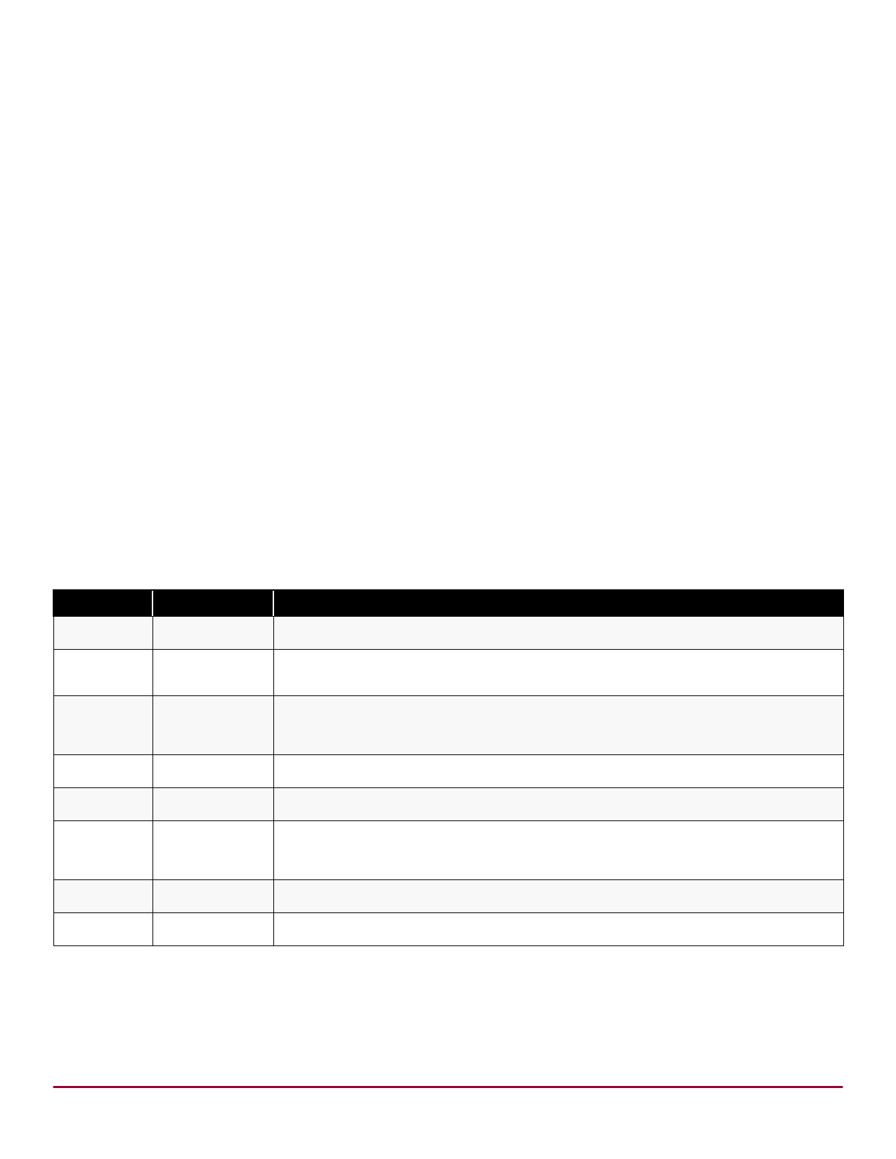
Pin Description
Pin #
Pin Name
1
IN
2
RA
3
LOAD
4
NC
5
NC
6
OUT
7
NC
8
GND
Description
Sense amplifier input and supply.
Provides gain setting of the transconductance amplifier. Connect gain setting resistor
(RA) between Pin 1 and Pin 2.
Sense amplifier input. High impedance input with Zener diode protection. Add an
external protection resistor in series with LOAD if VSENSE exceeds the range of -600mV
to +5.0V.
No Connect. This pin must be left floating for proper operation
No Connect. This pin must be left floating for proper operation.
Output of the transconductance amplifier. Output current to output voltage conversion
can be accomplished through addition of an external resistor (RB) at this pin. Overall
voltage gain is determined by the ratio of RB to RA.
No Connect. This pin must be left floating for proper operation.
Supply return.
Doc.# DSFP-HV7802
A062813
Supertex inc.
4
www.supertex.com
Share Link: 