HV9912 查看數據表(PDF) - Supertex Inc
零件编号
产品描述 (功能)
生产厂家
HV9912 Datasheet PDF : 12 Pages
| |||
HV9912
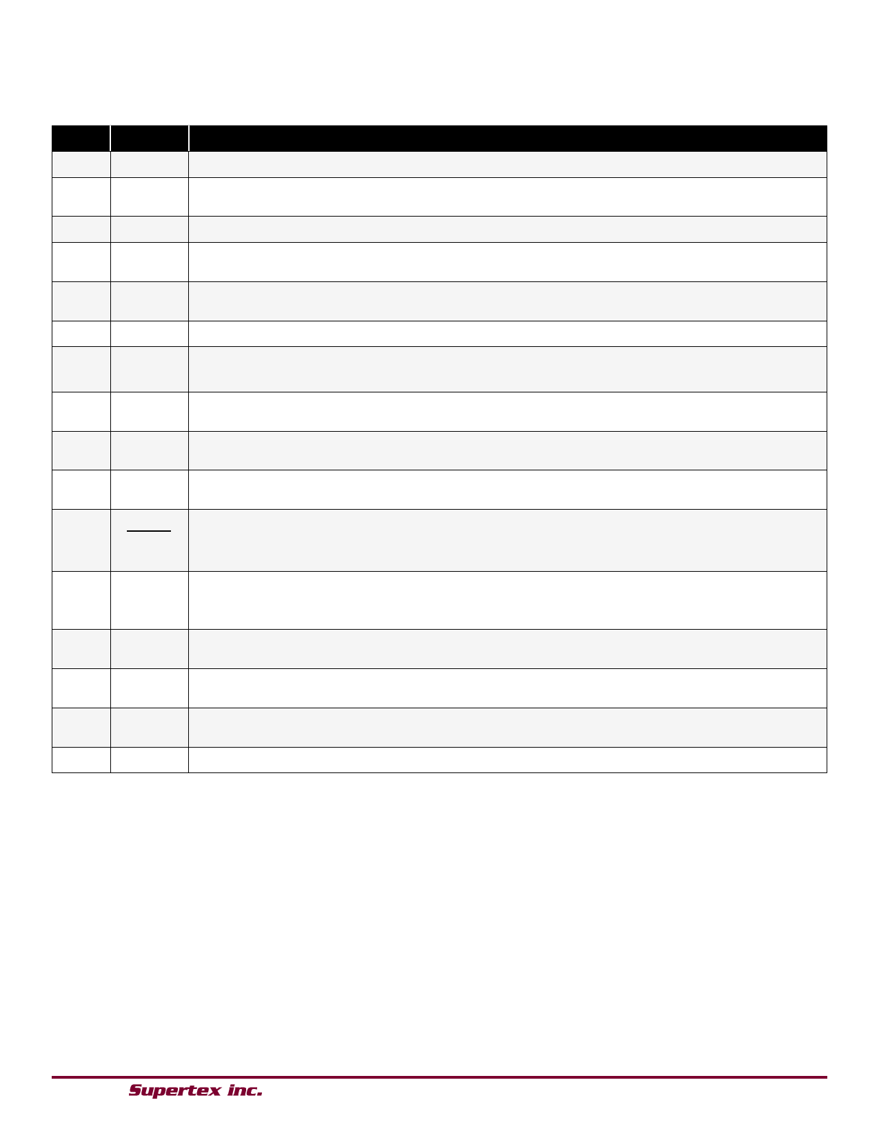
Pin Description
Pin #
Pin Description
1
VIN This pin is the input of a 90V high voltage regulator.
2
VDD
This is a power supply pin for all internal circuits. It must be bypassed with a low ESR capacitor to
GND (at least 0.1µF).
3
GATE This pin is the output gate driver for an external N-channel power MOSFET.
4
GND
Ground return for all the low power analog internal circuitry. This pin must be connected to the return
path from the input.
5
CS
This pin is used to sense the source current of the external power FET. It includes a built-in 100ns
(min) blanking time.
6
SC This pin is used to set the slope compensation.
7
RT
This pin sets the frequency of the power circuit. A resistor between RT and GND will program the
circuit in constant frequency mode.
8
SYNC
This I/O pin may be connected to the SYNC pin of other HV9912 circuits and will cause the oscillators
to lock to the highest frequency oscillator.
9
CLIM
This pin provides a programmable input current limit for the converter. The current limit can be set
by using a resistor divider from the REF pin.
10
REF
This pin provides 2% accurate reference voltage. It must be bypassed with a 0.01μF – 0.1μF
capacitor to GND.
This pin is pulled to ground when there is an output short circuit condition or output over voltage
11
FAULT condition. This pin can be used to drive an external MOSFET in the case of boost converters to
disconnect the load from the source.
This pin provides the over voltage protection for the converter. When the voltage at this pin exceeds
12
OVP 5V, the gate output of the HV9912 is turned off and FLT goes low. The IC will turn on when the
voltage at the pin goes below 4.5V.
13
PWMD
When this pin is pulled to GND (or left open), switching of the HV9912 is disabled. When an external
TTL high level is applied to it, switching will resume.
14
COMP
Stable Closed loop control can be accomplished by connecting a compensation network between
COMP and GND. This capacitor also controls the hiccup time.
15
IREF
The voltage at this pin sets the output current level. The current reference can be set using a resistor
divider from the REF pin.
16
FDBK This pin provides output current feedback to the HV9912 by using a current sense resistor.
● 1235 Bordeaux Drive, Sunnyvale, CA 94089 ● Tel: 408-222-8888 ● www.supertex.com
11
Share Link: 