HV9912 查看數據表(PDF) - Supertex Inc
零件编号
产品描述 (功能)
生产厂家
HV9912 Datasheet PDF : 12 Pages
| |||
HV9912
The VDD pin must be bypassed by a low ESR capacitor
(≥0.1µF) to provide a low impedance path for the high fre-
quency current of the output gate driver.
The input current drawn from the VIN pin is a sum of the
1.5mA current drawn by the internal circuit and the current
drawn by the gate driver (which in turn depends on the switch-
ing frequency and the gate charge of the external FET).
IIN = 1.5mA + (QG x fS)
(Eqn. 1)
In the above equation, fs is the switching frequency and QG
is the gate charge of the external FET (which can be ob-
tained from the datasheet of the FET).
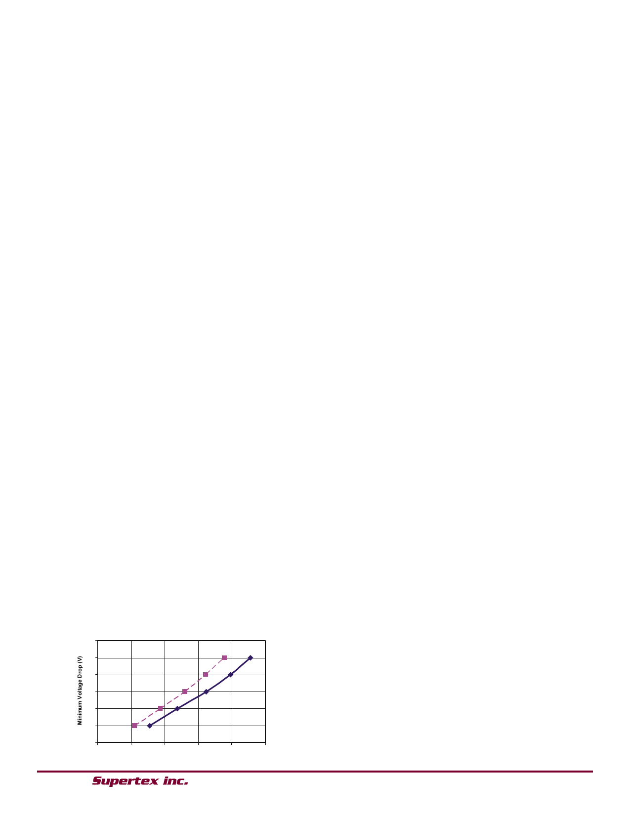
Minimum Input Voltage at VIN pin
The minimum input voltage at which the converter will start
and stop depends on the minimum voltage drop required for
the linear regulator. The internal linear regulator will regulate
the voltage at the VDD pin when VIN is between 9V and 90V.
However, when VIN is less than 9V, the converter will still
function as long as VDD is greater than the under voltage
lockout. Thus, the converter might be able to start at lower
than 9V. The start/stop voltages at the VIN pin can be deter-
mined using the minimum voltage drop across the linear reg-
ulator as a function of the current drawn. This data is shown
in Fig. 1 for ambient temperatures of 25ºC and 85ºC.
In this case, the gate drive draws too much current and
VINSTART is less than VINSTOP. In such cases, the IC will oscil-
late between ON and OFF if the input voltage is between the
start and stop voltages. In these circumstances, it is recom-
mended that the input voltage be kept higher than VINSTOP.
Reference
HV9912 includes a 2% accurate, 1.25V reference, which
can be used as the reference for the output current as well
as to set the switch current limit. The reference is buffered
so that it can deliver a maximum of 500µA external current
to drive the external circuitry. The reference should be by-
passed with at least a 10nF low ESR capacitor.
Note: In order to avoid abnormal start-up conditions, the by-
pass capacitor at the REF pin should not exceed 0.1μF.
Oscillator
Connecting a resistor between RT and GND will program the
time period.
In both cases, resistor RT sets the current which charges
an internal oscillator capacitor. The capacitor voltage ramps
up linearly and when the voltage increases beyond the
internal set voltage, a comparator triggers the SET input of
the internal SR flip-flop. This starts the next switching cycle.
The time period of the oscillator can be computed as:
Assume an ambient temperature of 85OC. Assuming the IC
is driving a 15nC gate charge FET at 200kHz, the total input
current is estimated to be 4.5mA (using Eqn. 1). At this input
current, the minimum voltage drop from Fig. 1 can be ap-
proximately estimated to be VDROP = 1.25V. However, before
the IC starts switching the current drawn will be 1.5mA. At
this current level, the voltage drop is approximately VDROP1 =
0.3V. Thus, the start/stop VIN voltages can be computed to
be:
VINSTART = UVLOMAX + VDROP1
= 7.0V + 0.3V
(Eqn. 2)
= 7.3V
VINSTOP = UVLOMAX - ΔUVLO + VDROP
= 7.0V - 0.5V + 1.25V
= 7.75V
Fig. 1 Headroom vs Input Current
Minimum Voltage Drop vs. IIN
3
2.5
2
TA = 85OC
1.5
TA = 25OC
1
0.5
0
0
2
4
6
8
10
IIN (mA)
TS ≈ RT x 18pF
(Eqn. 3)
Synchronization
The SYNC pin is an input/output (I/O) port to a fault toler-
ant peer-to-peer and/or master clock synchronization circuit.
For synchronization, the SYNC pins of multiple HV9912
based converters can be connected together and may also
be connected to the open drain output of a master clock.
When connected in this manner, the oscillators will lock to
the device with the highest operating frequency. When syn-
chronizing multiple ICs, it is recommended that the same
timing resistor be (corresponding to the switching frequency)
be used in all the HV9912 circuits.
In rare occasions, given the length of the connecting lines for
the SYNC pins, a resistor between SYNC and GND may be
required to damp any ringing due to parasitic capacitances.
It is recommended that the resistor chosen be greater than
300kΩ.
When synchronized in this manner, a permanent HIGH or
LOW condition on the SYNC pin will result in a loss of syn-
chronization, but the HV9912 based converters will continue
to operate at their individually set operating frequency. Since
loss of synchronization will not result in total system failure,
the SYNC pin is considered fault tolerant.
● 1235 Bordeaux Drive, Sunnyvale, CA 94089 ● Tel: 408-222-8888 ● www.supertex.com
6
Share Link: 