HV9982K6-G 查看數據表(PDF) - Supertex Inc
零件编号
产品描述 (功能)
生产厂家
HV9982K6-G Datasheet PDF : 13 Pages
| |||
HV9982
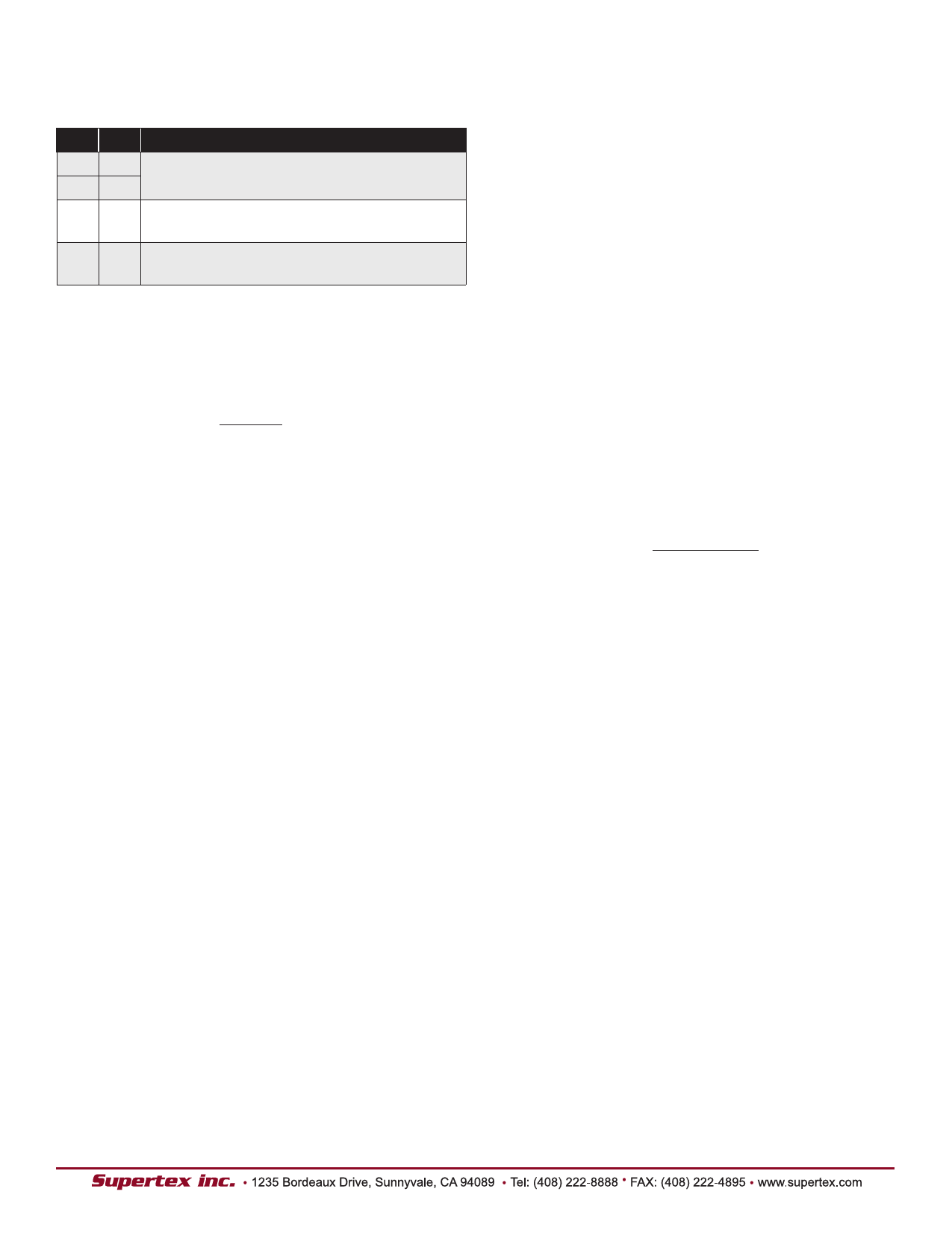
Table 1: S1 and S2 control logic
S1 S2 PWMD output
00
The output will follow PWMD input signal
01
1
0
Input DC zero volt corresponds to 100% duty
cycle output
1
1
Input DC two volt corresponds to 100% duty
cycle output
When S1 is high and the HV9982 is operating in the analog
control of PWM dimming mode, the PWM dimming frequen-
cy is set by a capacitor connected at the RAMP pin. The
RAMP frequency range is 100Hz - 1.0kHz and the capacitor
can be selected as:
f(Hz) = 1.0µS
C
RAMP
(Note: In the following description of the PWM dimming
performance the PWMD signals refer to the internal
PWM dimming signal and not to the signal applied at
the PWMD pins).
When the PWM signal is high, the GATE and FLT pins are
enabled and the output of the transconductance opamp is
connected to the external compensation network. Thus,
the internal amplifier controls the output current. When the
PWMD signal goes low, the output of the transconductance
amplifier is disconnected from the compensation network.
Thus, the integrating capacitor maintains the voltage across
it. The GATE is disabled, so the converter stops switching
and the FLT pin goes low, turning off the disconnect switch.
The output capacitor of the converter determines the PWM
dimming response of the converter, since it has to get
charged and discharged whenever the PWMD signal goes
high or low. In the case of a buck converter, since the in-
ductor current is continuous, a very small capacitor is used
across the LEDs. This minimizes the effect of the capacitor
on the PWM dimming response of the converter. However,
in the case of a boost converter, the output current is dis-
continuous and a very large output capacitor is required to
reduce the ripple in the LED current. Thus, this capacitor will
have a significant impact on the PWM dimming response.
By turning off the disconnect switch when PWMD goes low,
the output capacitor is prevented from being discharged and
thus the PWM dimming response of the boost converter Im-
proves dramatically.
Fault Conditions
The HV9982 is a robust controller which can protect the
LEDs and the LED driver in case of fault conditions. The
HV9982 includes both open LED protection and output short
circuit protection. In both cases, the HV9982 shuts down
and attempts a restart. The hiccup time can be programmed
by a single external capacitor at the SKIP pin.
During start-up or when a fault condition is detected, both
GATE and FLT outputs are disabled, the COMP pins and
SKIP pins are pulled to GND. Once the voltage at the SKIP
pin falls below 0.1V and the fault condition(s) have disap-
peared, the capacitor at the SKIP pin is released and is
charged slowly by a 10μA current source. Once the capacitor
is charged to 5.0V, the COMP pins are released and GATE
and FLT pins are allowed to turn on. If the hiccup time is long
enough, it will ensure that the compensation networks are
all completely discharged and that the converters start at
minimum duty cycle.
The hiccup timing capacitor can be programmed as:
CRAMP =
10µA • tHICCUP
4.9V
Short Circuit Protection
When a short circuit condition is detected (output current be-
comes higher than twice the steady state current), the GATE
and FLT outputs are pulled low. As soon as the disconnect
FET is turned off, the output current goes to zero and the
short circuit condition disappears. At this time, the hiccup
timer is started (Fig. 3). Once the timing is complete, the
converter attempts to restart. If the fault condition still per-
sists, the converter shuts down and goes through the cycle
again. If the fault condition is cleared (due to a momentary
output short) the converter will start regulating the output
current normally. This allows the LED driver to recover from
accidental shorts without having to reset the IC.
During short circuit conditions, there are two conditions that
determine the hiccup time.
The first is the time required to discharge the compensation
capacitors. Assuming a pole-zero R-C network at the COMP
pin (series combination of RZ and CZ in parallel with CC),
tCOMP,n = 3 • RZn • CZn
Note that disconnecting the LED load during PWM dimming
causes the energy stored in the inductor to be dumped into
the output capacitor. The filter capacitor should be chosen
large enough so that it can absorb the inductor energy with-
out significant change to the voltage across it.
where n refers to the channel number.
In case the compensation networks are only type 1 (single
capacitor), then:
tCOMP,n = 3 • 300Ω • CZn
8
Share Link: 