IDT54FCT162652AT 查看數據表(PDF) - Integrated Device Technology
零件编号
产品描述 (功能)
生产厂家
IDT54FCT162652AT Datasheet PDF : 9 Pages
| |||
IDT54/74FCT16652T/AT/CT/ET, FCT162652T/AT/CT/ET
FAST CMOS 16-BIT BUS TRANSCEIVER/REGISTER
MILITARY AND COMMERCIAL TEMPERATURE RANGES
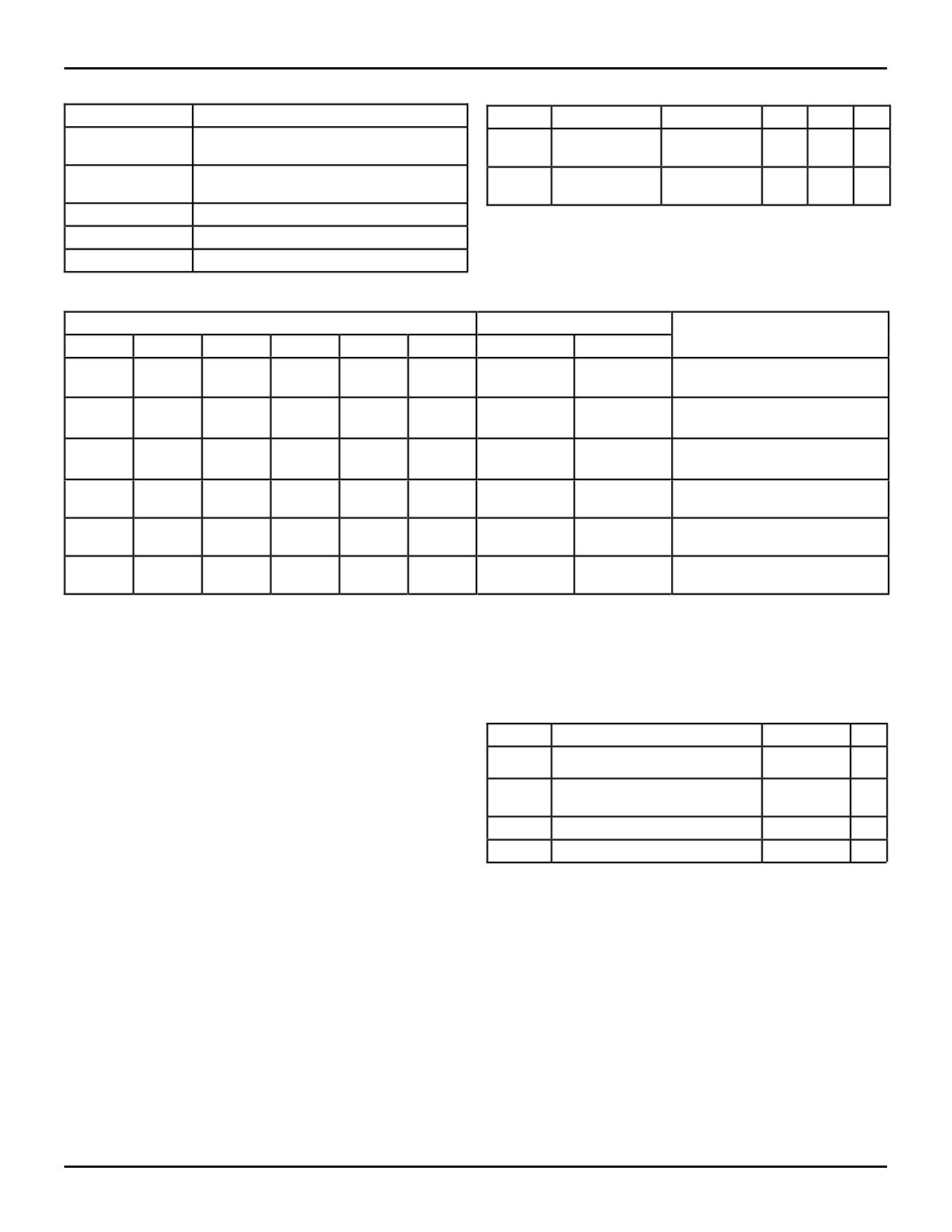
PIN DESCRIPTION
CAPACITANCE (TA = +25°C, f = 1.0MHz)
Pin Names
Description
xAx
Data Register A Inputs
Data Register B Outputs
xBx
Data Register B Inputs
Data Register A Outputs
xCLKAB, xCLKBA Clock Pulse Inputs
xSAB, xSBA Output Data Source Select Inputs
xOEAB, xOEBA Output Enable Inputs
Symbol Parameter(1) Conditions Typ. Max. Unit
CIN
Input
VIN = 0V
4.5 6.0 pF
Capacitance
CI/O
I/O
VOUT = 0V 5.5 8.0 pF
Capacitance
NOTE:
2549 lnk 02
1. This parameter is measured at characterization but not tested.
FUNCTION TABLE(2)
2549 tbl 01
Inputs
xOEAB xOEBA xCLKAB xCLKBA xSAB
xSBA
Data I/O(1)
xAx
xBx
Operation or Function
L
H
H or L H or L
X
X
Input
L
H
↑
↑
X
X
Input
Isolation
Store A and B Data
X
H
↑
H or L
X
X
H
H
↑
↑
X(2)
X
Input
Input
Unspecified(1) Store A, Hold B
Output Store A in Both Registers
L
X
H or L
↑
X
X
Unspecified(1)
Input
Hold A, Store B
L
L
↑
↑
X
X(2)
Output
Input
Store B in both Registers
L
L
X
X
X
L
Output
Input
Real Time B Data to A Bus
L
L
X
H or L
X
H
Stored B Data to A Bus
H
H
X
X
L
X
Input
Output Real Time A Data to B Bus
H
H
H or L
X
H
X
Stored A Data to B Bus
H
L
H or L H or L
H
H
Output
Output Stored A Data to B Bus and
Stored B Data to A Bus
NOTES:
1. The data output functions may be enabled or disabled by various signals at the xOEAB or xOEBA inputs.
2549 tbl 03
Data input functions are always enabled, i.e. data at the bus pins will be stored on every LOW-to-HIGH
transition on the clocks inputs.
2. Select control = L: clocks can occur simultaneously.
Select control = H: clocks must be staggered to load both registers.
3. H = HIGH Voltage Level
L = LOW Voltage Level
X = Don't care
↑ = LOW-to-HIGH Transition
ABSOLUTE MAXIMUM RATINGS(1)
Symbol
Description
Max. Unit
VTERM(2) Terminal Voltage with Respect to –0.5 to +7.0 V
GND
VTERM(3) Terminal Voltage with Respect to –0.5 to
V
GND
VCC +0.5
TSTG Storage Temperature
–65 to +150 °C
IOUT DC Output Current
–60 to +120 mA
NOTES:
2549 lnk 04
1. Stresses greater than those listed under ABSOLUTE MAXIMUM RAT-
INGS may cause permanent damage to the device. This is a stress rating
only and functional operation of the device at these or any other conditions
above those indicated in the operational sections of this specification is
not implied. Exposure to absolute maximum rating conditions for
extended periods may affect reliability.
2. All device terminals except FCT162XXXT Output and I/O terminals.
3. Output and I/O terminals for FCT162XXXT.
3
Share Link: 