IDT7006S17FB 查看數據表(PDF) - Integrated Device Technology
零件编号
产品描述 (功能)
生产厂家
IDT7006S17FB Datasheet PDF : 20 Pages
| |||
IDT7006S/L
HIGH-SPEED 16K x 8 DUAL-PORT STATIC RAM
MILITARY AND COMMERCIAL TEMPERATURE RANGES
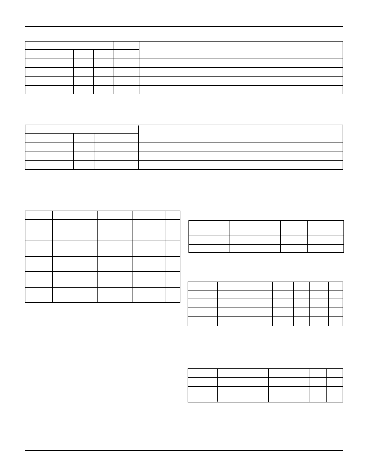
TRUTH TABLE I – NON-CONTENTION READ/WRITE CONTROL
Inputs(1)
Outputs
CE
R/W OE SEM I/O0-7
Mode
H
X
X
H High-Z
Deselected: Power-Down
L
L
X
H DATAIN
Write to Memory
L
H
L
H DATAOUT
Read Memory
X
X
H
X High-Z
Outputs Disabled
NOTE:
1. A0L — A13L is not equal to A0R — A13R.
2739 tbl 02
TRUTH TABLE II – SEMAPHORE READ/WRITE CONTROL(1)
Inputs
Outputs
CE
R/W OE SEM I/O0-7
Mode
H
H
L
L DATAOUT
Read Data in Semaphore Flag Data Out
H
u
X
L DATAIN
Write I/O0 into Semaphore Flag
L
X
X
L
—
Not Allowed
NOTE:
1. There are eight semaphore flags written to via I/O0 and read from I/O0 - I/O15. These eight semaphores are addressed by A0 - A2.
2739 tbl 03
ABSOLUTE MAXIMUM RATINGS(1)
Symbol
Rating
Commercial Military Unit
VTERM(2) Terminal Voltage –0.5 to +7.0 –0.5 to +7.0 V
with Respect
to GND
TA
Operating
0 to +70 –55 to +125 °C
Temperature
TBIAS
Temperature
Under Bias
–55 to +125 –65 to +135 °C
TSTG
Storage
Temperature
–55 to +125 –65 to +150 °C
IOUT
DC Output
Current
50
50
mA
NOTES:
2739 tbl 04
1. Stresses greater than those listed under ABSOLUTE MAXIMUM
RATINGS may cause permanent damage to the device. This is a stress
rating only and functional operation of the device at these or any other
conditions above those indicated in the operational sections of this
specification is not implied. Exposure to absolute maximum rating condi-
tions for extended periods may affect reliability.
2. VTERM must not exceed Vcc + 0.5V for more than 25% of the cycle time
or 10ns maximum, and is limited to < 20mA for the period of VTERM < Vcc
+ 0.5V.
RECOMMENDED OPERATING
TEMPERATURE AND SUPPLY VOLTAGE
Grade
Ambient
Temperature
GND
VCC
Military
–55°C to +125°C
0V
5.0V ± 10%
Commercial
0°C to +70°C
0V
5.0V ± 10%
2739 tbl 05
RECOMMENDED DC OPERATING
CONDITIONS
Symbol
Parameter
Min. Typ.
VCC
Supply Voltage
4.5 5.0
GND Supply Voltage
0
0
VIH
Input High Voltage
2.2 —
VIL
Input Low Voltage –0.5(1) —
NOTES:
1. VIL≥ -1.5V for pulse width less than 10ns.
2. VTERM must not exceed Vcc + 0.5V.
Max. Unit
5.5 V
0V
6.0(2) V
0.8 V
2739 tbl 06
CAPACITANCE(1)
(TA = +25°C, f = 1.0MHz)TQFP PACKAGE
Symbol
Parameter
Conditions(2) Max. Unit
CIN
Input Capacitance VIN = 3dV
9
pF
COUT
Output
Capacitance
VOUT = 3dV
10
pF
NOTES:
2739 tbl 07
1. This parameter is determined by device characterization, but is not
production tested.
2. 3dv references the interpolated capacitance when the input and output
signals switch from 0V to 3V or from 3V to 0V.
6.07
4
Share Link: 