IDT7006S17F 查看數據表(PDF) - Integrated Device Technology
零件编号
产品描述 (功能)
生产厂家
IDT7006S17F Datasheet PDF : 20 Pages
| |||
IDT7006S/L
HIGH-SPEED 16K x 8 DUAL-PORT STATIC RAM
MILITARY AND COMMERCIAL TEMPERATURE RANGES
DC ELECTRICAL CHARACTERISTICS OVER THE
OPERATING TEMPERATURE AND SUPPLY VOLTAGE RANGE(1)(Cont'd.) (VCC = 5.0V ± 10%)
Symbol
ICC
ISB1
ISB2
ISB3
ISB4
Parameter
Dynamic Operating
Current
(Both Ports Active)
Standby Current
(Both Ports — TTL
Level Inputs)
Standby Current
(One Port — TTL
Level Inputs)
Full Standby Current
(Both Ports — All
CMOS Level Inputs)
SEMR = SEML≥ VCC-0.2V
Full Standby Current
(One Port — All
CMOS Level Inputs)
Test
Condition
Version
CE = VIL, Outputs Open MIL.
S
SEM = VIH
L
f = fMAX(3)
COM’L. S
L
CEL = CER = VIH
SEMR = SEML = VIH
MIL.
S
L
f = fMAX(3)
COM’L. S
L
CE CE "A"=VIL and L"B"=VIH(5) MIL.
S
Active Port Outputs Open,
L
f = fMAX(3)
COM’L. S
SEMR = SEML = VIH
L
Both Ports CEL and
CER > VCC - 0.2V
MIL.
S
L
VIN > VCC - 0.2V or
VIN < 0.2V, f = 0(4)
COM’L. S
L
CE"A" < 0.2V and
MIL.
S
CE"B" > VCC - 0.2V(5)
SEMR = SEML≥ VCC - 0.2V
L
VIN > VCC - 0.2V or
COM’L. S
VIN < 0.2V
Active Port Outputs Open,
L
f = fMAX(3)
7006X35
Typ.(2)
150
140
150
140
13
10
13
10
85
75
85
75
1.0
0.2
1.0
0.2
Max.
300
250
250
210
80
65
60
50
190
160
155
130
30
10
15
5
80 175
70 150
80 135
70 110
7006X55
7006X70
Mil Only
Typ.(2) Max. Typ.(2) Max. Unit
150 300 140 300 mA
140 250 130 250
150 250 — —
140 210 — —
13 80 10 80 mA
10 65
8
65
13 60 — —
10 50 — —
85 190 80 190 mA
75 160 70 160
85 155 — —
75 130 — —
1.0 30 1.0 30 mA
0.2 10 0.2 10
1.0 15 — —
0.2 5
——
80 175 75 175 mA
70 150 65 150
80 135 — —
70 110 — —
NOTES:
2739 tbl 10
1. "X" in part numbers indicates power rating (S or L).
2. VCC = 5V, TA = +25°C, and are not production tested. ICC DC =120mA (typ).
3. At f = fMAX, address and I/O'S are cycling at the maximum frequency read cycle of 1/tRC, and using “AC Test Conditions” of input levels of GND to 3V.
4. f = 0 means no address or control lines change.
5. Port "A" may be either left or right port. Port "B"is the opposite from port "A".
DATA RETENTION CHARACTERISTICS OVER ALL TEMPERATURE RANGES (L Version Only)
(VLC = 0.2V, VHC = VCC - 0.2V)(4)
Symbol
Parameter
Test Condition
Min.
Typ.(1)
Max. Unit
VDR
ICCDR
tCDR(3)
tR(3)
VCC for Data Retention
Data Retention Current
Chip Deselect to Data Retention Time
Operation Recovery Time
VCC = 2V
CE ≥ VHC
VIN ≥ VHC or ≤ VLC
SEM ≥ VHC
MIL.
COM’L.
2.0
—
—
0
tRC(2)
—
—
V
100
4000 µA
100
1500
—
—
ns
—
—
ns
NOTES:
1. TA = +25°C, VCC = 2V, and are not production tested.
2. tRC = Read Cycle Time
3. This parameter is guaranteed by characterization, but are not production tested.
4. At Vcc = 2V input leakages are undefined
2739 tbl 11
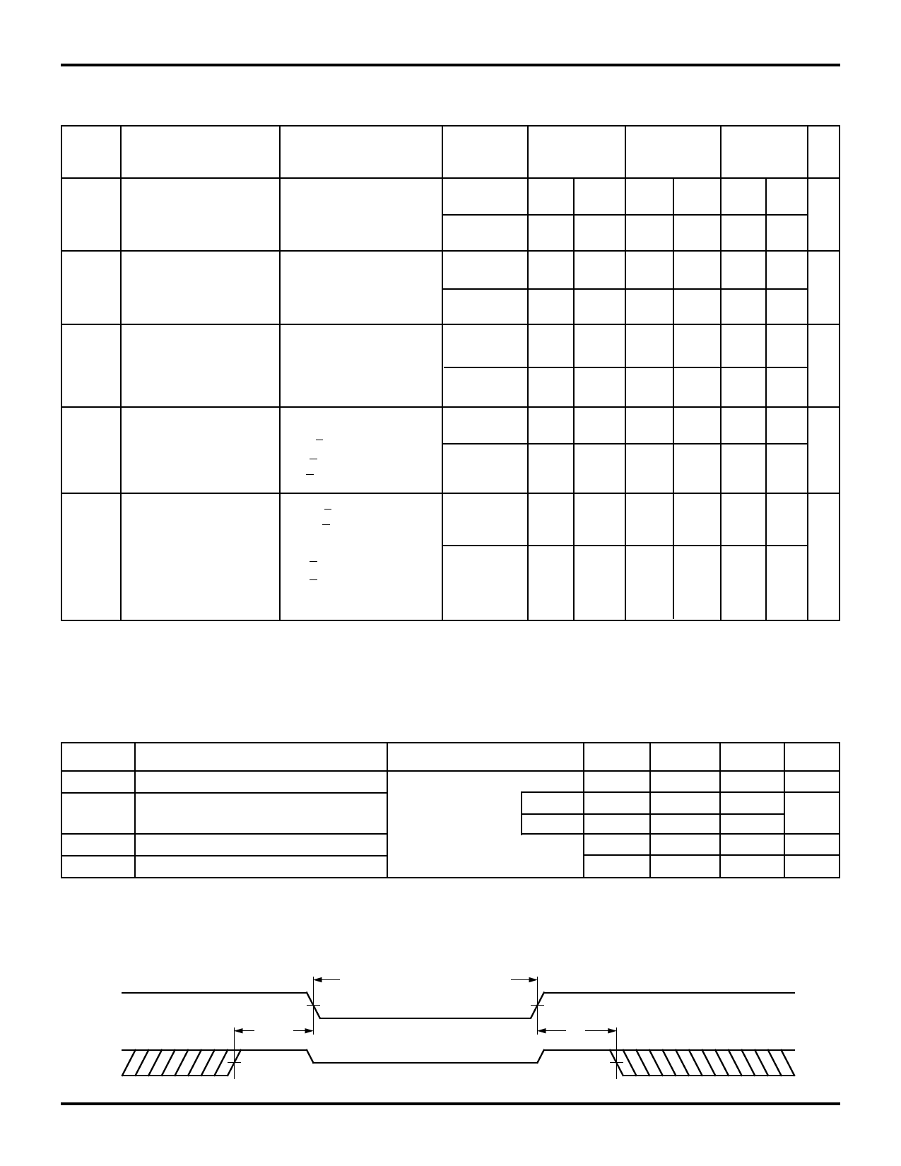
DATA RETENTION WAVEFORM
VCC
4.5V
tCDR
CE
VIH
DATA RETENTION MODE
VDR ≥ 2V
VDR
4.5V
tR
VIH
2739 drw 05
6.07
6
Share Link: 