IDT72V3611 查看數據表(PDF) - Integrated Device Technology
零件编号
产品描述 (功能)
生产厂家
IDT72V3611 Datasheet PDF : 20 Pages
| |||
IDT72V3611 3.3V, CMOS SyncFIFOTM
64 x 36
COMMERCIAL TEMPERATURE RANGE
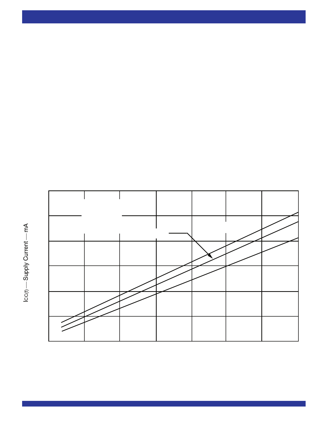
DETERMINING ACTIVE CURRENT CONSUMPTION AND POWER DISSIPATION
The ICC(f) data for the graph was taken while simultaneously reading and writing the FIFO on the IDT72V3611 with CLKA and CLKB operating at frequency
fS. All data inputs and data outputs change state during each clock cycle to consume the highest supply current. Data outputs were disconnected to normalize
the graph to a zero-capacitance load. Once the capacitance load per data-output channel is known, the power dissipation can be calculated with the equation
below.
CALCULATING POWER DISSIPATION
With ICC(f) taken from Figure 1, the maximum power dissipation (PT) of the IDT72V3611 may be calculated by:
PT = VCC x ICC(f) + Σ(CL x (VOH - VOL)2 x fO)
N
where:
N
=
number of outputs = 36
CL
=
output capacitance load
fO
=
switching frequency of an output
VOH =
output high-level voltage
VOL =
output low-level voltage
When no read or writes are occurring on this device, the power dissipated by a single clock (CLKA or CLKB) input running at frequency fS is
calculated by:
PT = VCC x fS x 0.025 mA/MHz
150
fdata = 1/2 fS
125
TA = 25 C
CL = 0 pF
VCC = 3.3V
100
75
VCC = 3.6V
VCC = 3.0V
50
25
0
0
10
20
30
40
50
fS Clock Frequency MHz
60
70
4657 drw 04
Figure 1. Typical Characteristics: Supply Current (ICC) vs. Clock Frequency (fS)
7
Share Link: 