IMP2524-1BN 查看數據表(PDF) - A1 PROs co., Ltd.
零件编号
产品描述 (功能)
生产厂家
IMP2524-1BN Datasheet PDF : 32 Pages
| |||
IMP2524/27
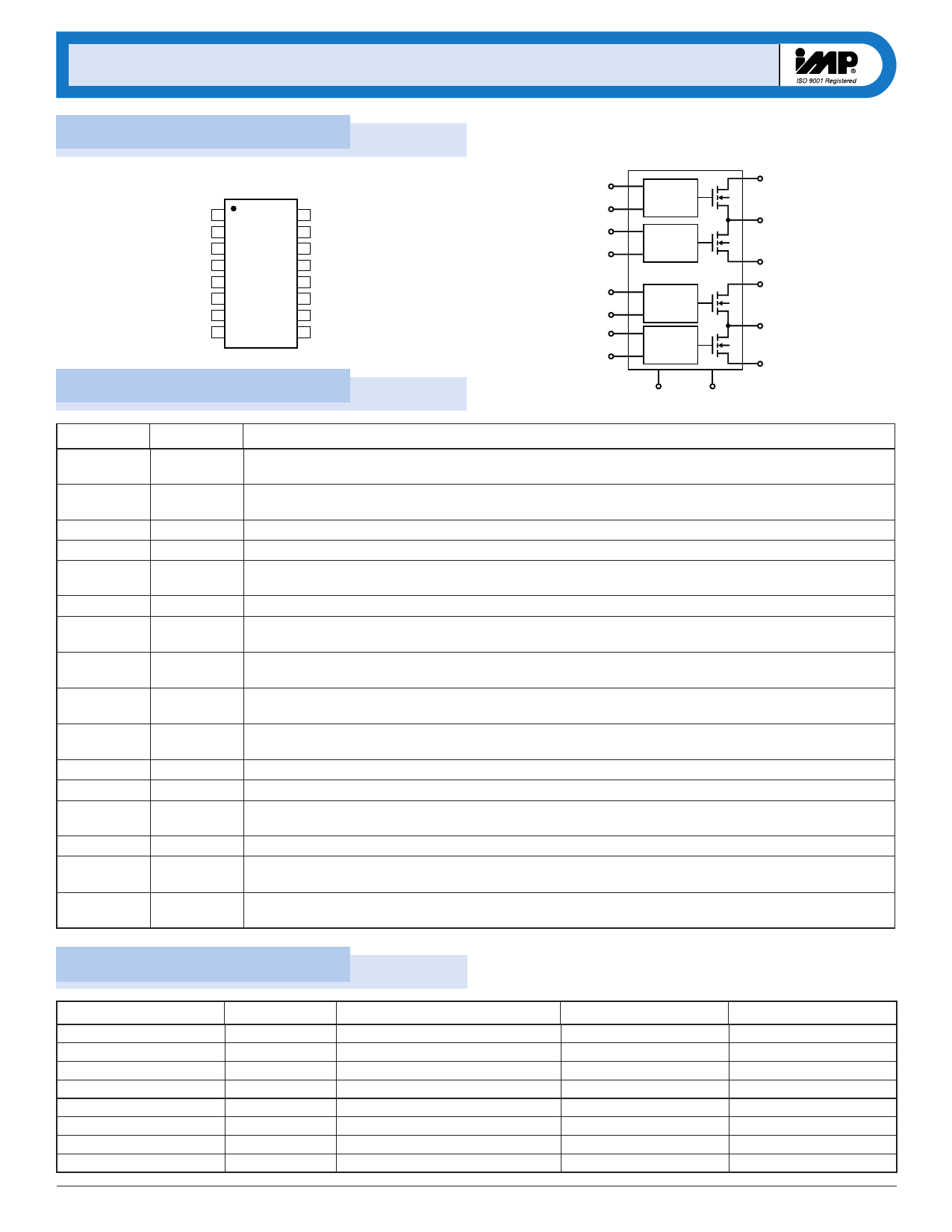
Pin Configuration
SO/DIP
FLGA 1
ENA 2
OUTA 3
GND 4
INC/D 5
OUTC 6
ENC 7
FLGC 8
16 FLGB
15 ENB
IMP2524/27 14 OUTB
13 INA/B
12 GND
11 OUTD
10 END
9 FLGD
2524/27_02.eps
Pin Descriptions
1
FLGA
2
ENA
FLGB 16
ENB 15
ENC 7
FLGC 8
FLGD 9
END 10
Logic,
Charge
Pump
Logic,
Charge
Pump
IMP2524/27
Logic,
Charge
Pump
Logic,
Charge
Pump
4
GND
12
GND
3
OUTA
13
INA/B
14
OUTB
6
OUTC
5
INC/D
11
OUTD
2524/27_03.eps
Pin Number
1
2
3
4
5
6
7
8
9
10
11
12
13
14
15
16
Name
FLGA
ENA
OUTA
GND
INC/D
OUTC
ENC
FLGC
FLGD
END
OUTD
GND
INA/B
OUTB
ENB
FLGB
Function
Fault Flag A output. This open-drain output goes into an active-LOW state in response to under-
voltage, current limit or thermal shutdown conditions.
Enable A Input. This pin is the Channel B MOSFET switch driver control logic input. Both active-HIGH
(-1 suffix) and active-LOW (-2 suffix) logic devices are available.
Channel-A switch output (MOSFET Source). The output pin drives the load into ON and OFF states.
Ground. Power supply return for the internal circuitry of the IC. Connect both pins 4 and 6 together.
Channel C and D positive power supply input voltage. This is the switching MOSFET drain connection.
It is the channel C and channel D supply voltage input for the logic and the charge-pump circuit.
Channel-C switch output (MOSFET Source). The output pin drives the load into ON and OFF states.
Enable C Input. This pin is the Channel B MOSFET switch driver control logic input. Both active-HIGH
(-1 suffix) and active-LOW (-2 suffix) logic devices are available.
Fault Flag C output. This open-drain output goes into an active-LOW state in response to under-
voltage, current limit or thermal shutdown conditions.
Fault Flag D output. This open-drain output goes into an active-LOW state in response to under-
voltage, current limit or thermal shutdown conditions.
Enable D Input. This pin is the Channel B MOSFET switch driver control logic input. Both active-HIGH
(-1 suffix) and active-LOW (-2 suffix) logic devices are available.
Channel-D switch output (MOSFET Source). The output pin drives the load into ON and OFF states.
Ground. Power supply return for the internal circuitry of the IC. Connect both pins 4 and 6 together.
Channel A and B positive power supply input voltage. This is the switching MOSFET drain connection.
It is the channel A and channel B supply voltage input for the logic and the charge-pump circuit.
Channel-B switch output (MOSFET Source). The output pin drives the load into ON and OFF states.
Enable B Input. This pin is the Channel-B MOSFET switch driver control logic input. Both active-HIGH
(-1 suffix) and active-LOW (-2 suffix) logic devices are available.
Fault Flag B output. This open-drain output goes into an active-LOW state in response to under-
voltage, current limit or thermal shutdown conditions.
2524/27t01
Ordering Information
Pin Number
IMP2524-1BWM
IMP2524-2BWM
IMP2524-1BN
IMP2524-2BN
IMP2527-1BWM
IMP2527-2BWM
IMP2527-1BN
IMP2527-2BN
2
Enable Logic
Active HIGH
Active LOW
Active HIGH
Active LOW
Active HIGH
Active LOW
Active HIGH
Active LOW
Typical “ON” Resistance
100mΩ
100mΩ
100mΩ
100mΩ
200mΩ
200mΩ
200mΩ
200mΩ
Temperature Range
–40° C to +85° C
–40° C to +85° C
–40° C to +85° C
–40° C to +85° C
–40° C to +85° C
–40° C to +85° C
–40° C to +85° C
–40° C to +85° C
408-432-9100/www.impweb.com
Pins-Package
16-SO
16-SO
16-DIP
16-DIP
16-SO
16-SO
16-DIP
16-DIP
2524/27t02
© 2000 IMP, Inc. 6
Share Link: 