IMP2524-1BN 查看數據表(PDF) - A1 PROs co., Ltd.
零件编号
产品描述 (功能)
生产厂家
IMP2524-1BN Datasheet PDF : 32 Pages
| |||
IMP2525
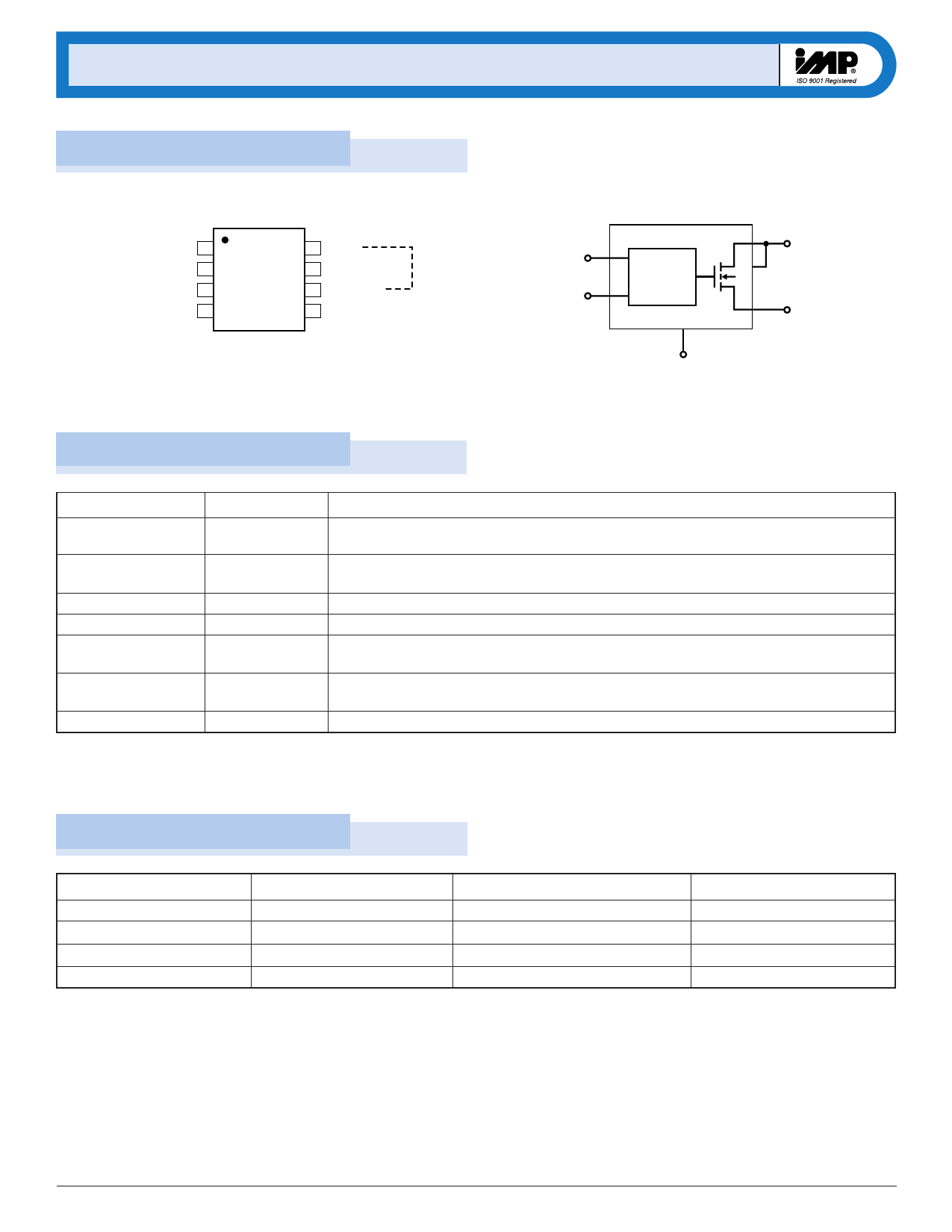
Pin Configuration
SO/DIP
EN 1
8 OUT
*
FLG 2 IMP2525 7 IN
GND 3
6 NC/OUT
NC 4
5 NC
*Connect pins 6 and 8 for MIC2525 compatibility
2525_02.eps
EN 1
2
FLG
Logic,
Charge
Pump
3
GND
8
OUT
6
7
IN
2525_03.eps
Pin Descriptions
Pin Number
1
2
3
4, 5
6
7
8
Name
EN
FLG
GND
NC
NC/OUT
IN
OUT
Function
Enable input. This pin is the MOSFET switch driver logic input. Both active-HIGH
(-1 suffix) and active-LOW (-2 suffix) logic devices are available.
Fault flag output. This open-drain output goes into an active-LOW state in response to
undervoltage, current limit or thermal shutdown conditions.
Ground. Power supply return for the internal circuitry of the IC.
No connection. These pins have no internal connections to the device.
No connection. This pin has no internal connection to the device. Connect pins 6 and 8 to
maintain pin-compatibility with the MIC2525.
Positive power supply voltage input. This is the switching MOSFET drain connection
as well as the positive supply for the IC.
MOSFET source. The output pin supplies power to the load.
Ordering Information
Part Number
IMP2525-1BM
IMP2525-2BM
IMP2525-1BN
IMP2525-2BN
Enable Logic
Active HIGH
Active LOW
Active HIGH
Active LOW
Temperature Range
– 40°C to +85°C
– 40°C to +85°C
– 40°C to +85°C
– 40°C to +85°C
Pins-Package
8-SO
8-SO
8-DIP
8-DIP
2
408-432-9100/www.impweb.com
© 2000 IMP, Inc. 6
Share Link: 