ST95020WM1TR 查看數據表(PDF) - STMicroelectronics
零件编号
产品描述 (功能)
生产厂家
ST95020WM1TR Datasheet PDF : 18 Pages
| |||
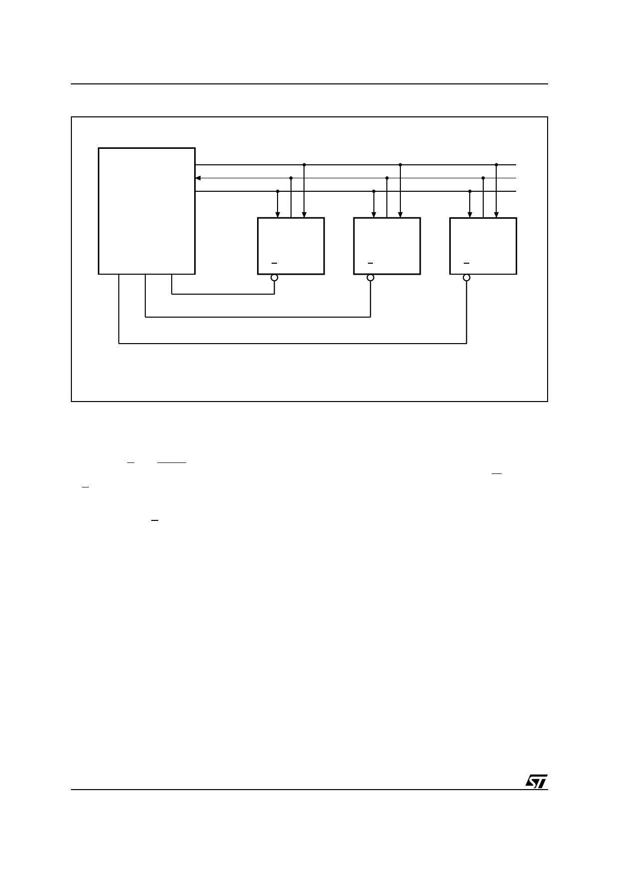
ST95040, ST95020, ST95010
Figure 12. EEPROM and SPI Bus
D
Q
C
MASTER
CS3 CS2 CS1
CQD
ST95xxx
S
CQD
ST95xxx
S
CQD
ST95xxx
S
AI01446
DATA PROTECTION AND PROTOCOL SAFETY
– All inputs are protected against noise, see Table
6.
– Non valid S and HOLD transitions are not taken
into account.
– S must come high at the proper clock count in
order to start a non-volatile write cycle (in the
memory array or in the status register), that is
the Chip Select S must rise during the clock pulse
following the introduction of a multiple of 8 bits.
– Access to the memory array during non-volatile
programming cycle is ignored; however, the pro-
gramming cycle continues.
– After any of the operations WREN, WRDI, RDSR
is completed, the chip enters a wait state and
waits for a deselect.
– The write enable latch is reset upon power-up.
– The write enable latch is reset when W is brought
low.
INITIAL DELIVERY STATE
The device is delivered with the memory array in a
fully erased state (all data set at all "1’s" or FFh).
The block protect bits are initialized to 00.
10/18
Share Link: 