IS25C16 查看數據表(PDF) - Integrated Silicon Solution
零件编号
产品描述 (功能)
生产厂家
IS25C16 Datasheet PDF : 14 Pages
| |||
IS25C08
IS25C16
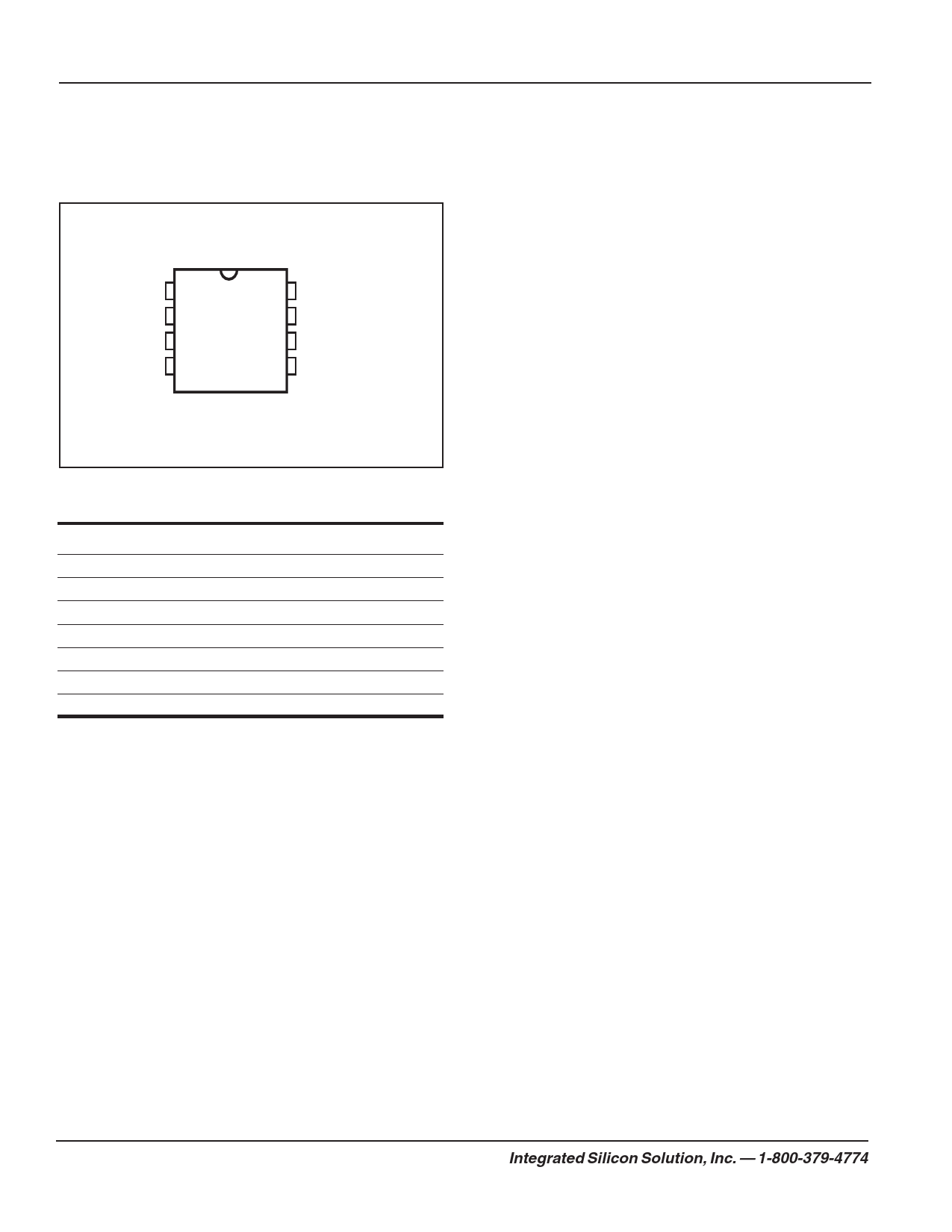
PIN CONFIGURATION
8-Pin DIP, SOIC, and TSSOP
CS 1
SO 2
WP 3
GND 4
8 VCC
7 HOLD
6 SCK
5 SI
ISSI ®
PIN DESCRIPTIONS
CS
SCK
SI
SO
GND
VCC
WP
HOLD
Chip Select
Serial Data Clock
Serial Data Input
Serial Data Output
Ground
Power
Write Protect
Suspends Serial Input
PIN DESCRIPTIONS
Serial Clock (SCK): This timing signal provides syn-
chronization between the microcontroller and IS25C08/
16. Op-Codes, byte addresses, and data are latched on
SI with a rising edge of the SCK. Data on SO is re-
freshed on the falling edge of SCK for SPI modes (0,0)
and (1,1).
Serial Data Input (SI): This is the input pin for all data
that the IS25C08/16 is required to receive.
Serial Data Output (SO): This is the output pin for all
data transmitted from the IS25C08/16.
Chip Select (CS): The CS pin activates the device.
Upon power-up, CS should follow Vcc. When the device
is to be enabled for instruction input, the signal requires
a High-to-Low transition. While CS is stable Low, the
master and slave will communicate via SCK, SI, and SO
signals. Upon completion of communication, CS must
be driven High. At this moment, the slave device may
start its internal write cycle. When CS is high, the
device enters a power-saving standby mode, unless an
internal write operation is underway. During this mode,
the SO pin becomes high impedance.
Write Protect (WP): The purpose of this input signal is
to initiate Hardware Write Protection mode. This mode
prevents the Block Protection bits and the WPEN bit in
the Status Register from being altered. To cause
Hardware Write Protection, WP must be Low at the same
time WPEN is 1. WP may be hardwired to Vcc or GND.
HOLD (HOLD): This input signal is used to suspend the
device in the middle of a serial sequence and temporarily
ignore further communication on the bus (SI, SO, SCK).
Together with Chip Select, the HOLD signal allows
multiple slaves to share the bus. The HOLD signal
transitions must occur only when SCK is Low, and be
held stable during SCK transitions. (See Figure 8 for
Hold timing) To disable this feature, HOLD may be
hardwired to Vcc.
2
Integrated Silicon Solution, Inc. — 1-800-379-4774
Preliminary Information Rev. 00H
02/23/06
Share Link: 