IS61NSCS25672 查看數據表(PDF) - Integrated Silicon Solution
零件编号
产品描述 (功能)
生产厂家
IS61NSCS25672 Datasheet PDF : 32 Pages
| |||
IS61NSCS25672
IS61NSCS51236
ISSI ®
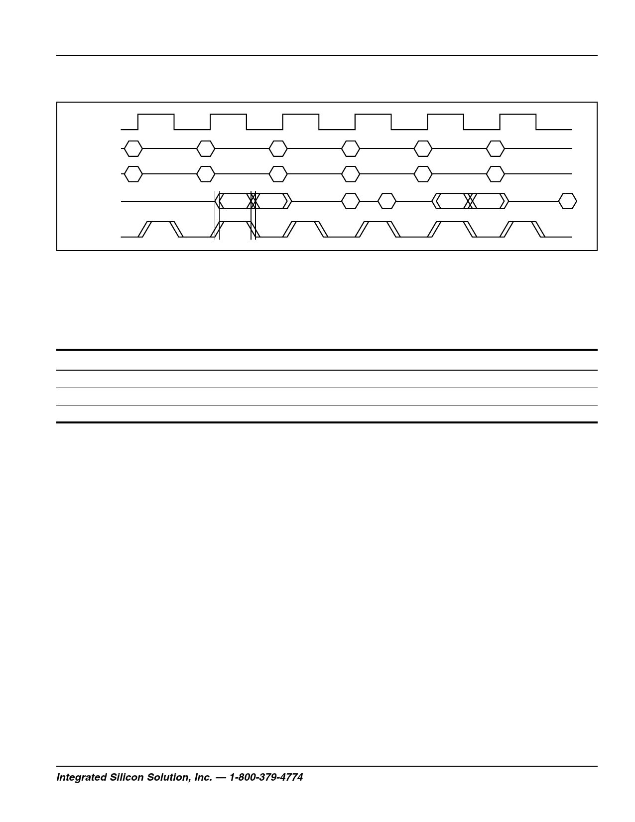
Double Data Rate Write—Double Data Rate Read (Σ1x2Lp). For reference only.
CK
Address A
Control R
DQ
CQ
B
C
D
E
F
X
W
R
X
W
QA0 QA1
DC0
DC1
QD0 QD1
DF0
Mode Selection Truth Table Standard
Name
M2 M3 M4
Function
Analogous to...
In This Data Sheet?
Σ1x2Lp
011
DDR
Double Data Rate SRAM
No
Σ1x1Dp
1 0 1 Double Late Write, Pipelined Read
Pipelined NBT SRAM
Yes
Σ1x1Lp
110
Late Write, Pipelined Read
Pipelined Late Write SRAM
No
Notes:
All address, data and control inputs (with the exception of EP2, EP3, and the mode pins, M2–M4) are synchronized to rising clock
edges. Read and write operations must be initiated with the Advance/Load pin (ADV) held low, in order to load the new address.
Device activation is accomplished by asserting all three of the Chip Enable inputs (E1, E2, and E3). Deassertion of any one of the
Enable inputs will deactivate the device. It should be noted that ONLY deactivation of the RAM via E2 and/or E3 deactivates the
Echo Clocks, CQ1–CQn.
READ OPERATIONS
Pipelined Read
Read operation is initiated when the following conditions
are satisfied at the rising edge of clock: All three chip
enables (E1, E2, and E3) are active, the write enable input
signal (W) is deasserted high, and ADV is asserted low.
The address presented to the address inputs is latched into
the address register and presented to the memory core
and control logic. The control logic determines that a read
access is in progress and allows the requested data to
propagate to the input of the output register. At the next
rising edge of clock the read data is allowed to propagate
through the output register and onto the output pins.
WRITE OPERATIONS
Write operation occurs when the following conditions are
satisfied at the rising edge of clock: All three chip enables
(E1, E2, and E3) are active and the write enable input
signal (W) is asserted low.
Double Late Write
Double Late Write means that Data In is required on the
third rising edge of clock. Double Late Write is used to
implement Pipeline mode NBT SRAMs.
Integrated Silicon Solution, Inc. — 1-800-379-4774
7
ADVANCE INFORMATION Rev. 00A
06/19/01
Share Link: 