IS93C46A 查看數據表(PDF) - Integrated Silicon Solution
零件编号
产品描述 (功能)
生产厂家
IS93C46A Datasheet PDF : 13 Pages
| |||
IS93C46A IS93C56A IS93C66A
ISSI ®
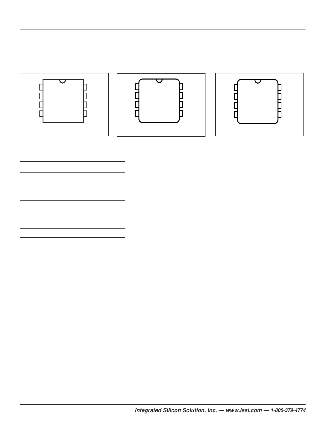
PIN CONFIGURATIONS
8-Pin DIP, 8-Pin TSSOP
CS 1
SK 2
DIN 3
DOUT 4
8 VDD
7 NC
6 ORG
5 GND
8-Pin JEDEC SOIC “G”
NC 1
VCC 2
CS 3
SK 4
8 ORG
7 GND
6 DOUT
5 DIN
(Rotated)
8-Pin JEDEC SOIC “GR”
CS 1
SK 2
DIN 3
DOUT 4
8 VCC
7 NC
6 ORG
5 GND
PIN DESCRIPTIONS
CS
SK
DIN
DOUT
ORG
NC
Vcc
GND
Chip Select
Serial Data Clock
Serial Data Input
Serial Data Output
Organization Select
Not Connected
Power
Ground
Applications
The IS93C46A/56A/66A is very popular in many high-
volume applications which require low-power, low-
density storage. Applications using this device
include industrial controls, networking, and numerous
other consumer electronics.
Endurance and Data Retention
The IS93C46A/56A/66A is designed for applications re-
quiring up to 1M programming cycles (WRITE, WRALL,
ERASE and ERAL). It provides 40 years of secure data
retention without power after the execution of 1M program-
ming cycles.
Device Operations
The IS93C46A/56A/66A are controlled by a set of
instructions which are clocked-in serially on the Din pin.
Before each low-to-high transition of the clock (SK), the
CS pin must have already been raised to HIGH, and the
Din value must be stable at either LOW or HIGH. Each
instruction begins with a start bit of the logical “1” or
HIGH. Following this are the opcode (2 bits),
address field (6, 7, 8, or 9 bits), and data, if
appropriate. The clock signal may be held stable at
any moment to suspend the device at its last state.
This allows clock-speed flexibility as well as
maximum power conservation.
Read (READ)
The READ instruction is the only instruction that outputs
serial data on the DOUT pin. After the read instruction and
address have been decoded, data is transferred from the
selected memory register into a serial shift register. (Please
note that one logical “0” bit precedes the actual 8 or 16-bit
output data string.) The output on DOUT changes during the
low-to-high transitions of SK (see Figure 3).
Low Voltage Read
The IS93C46A/56A/66A have been designed to ensure that
data read operations are reliable in low voltage environ-
ments. They provide accurate operation with Vcc as low
as 2.5V.
Auto Increment Read Operations
In the interest of memory transfer operation applications,
the IS93C46A/56A/66A has been designed to output a
continuous stream of memory content in response to a
single read operation instruction. To utilize this function, the
system asserts a read instruction specifying a start location
address. Once the 8 or16 bits of the addressed register have
been clocked out, the data in consecutively higher address
locations is output. The address will wrap around continu-
ously with CS HIGH until the chip select (CS) control pin is
brought LOW. This allows for single instruction data dumps
to be executed with a minimum of firmware overhead.
2
Integrated Silicon Solution, Inc. — www.issi.com — 1-800-379-4774
Rev. A
11/12/02
Share Link: 