K6E0808C1E-C 查看數據表(PDF) - Samsung
零件编号
产品描述 (功能)
生产厂家
K6E0808C1E-C Datasheet PDF : 9 Pages
| |||
K6E0808C1E-C/E-L, K6E0808C1E-I/E-P
For Cisco
CMOS SRAM
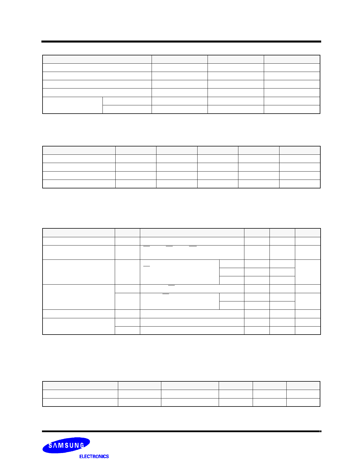
ABSOLUTE MAXIMUM RATINGS*
Parameter
Voltage on Any Pin Relative to VSS
Voltage on VCC Supply Relative to VSS
Power Dissipation
Storage Temperature
Operating Temperature Commercial
Industrial
Symbol
VIN, VOUT
VCC
PD
TSTG
TA
TA
Rating
-0.5 to 7.0
-0.5 to 7.0
1.0
-65 to 150
0 to 70
-40 to 85
Unit
V
V
W
°C
°C
°C
* Stresses greater than those listed under "Absolute Maximum Ratings" may cause permanent damage to the device. This is a stress rating only and
functional operation of the device at these or any other conditions above those indicated in the operating sections of this specification is not implied.
Exposure to absolute maximum rating conditions for extended periods may affect reliability.
RECOMMENDED DC OPERATING CONDITIONS*(TA=0 to 70°C)
Parameter
Supply Voltage
Ground
Input High Voltage
Input Low Voltage
Symbol
VCC
VSS
VIH
VIL
Min
4.5
0
2.2
-0.5**
Typ
Max
Unit
5.0
5.5
V
0
0
V
-
VCC+0.5***
V
-
0.8
V
* The above parameters are also guaranteed at industrial temperature range.
** VIL(Min) = -2.0(Pulse Width≤7ns) for I≤20mA.
*** VIH(Max) = VCC+2.0V(Pulse Width≤7ns) for I≤20mA.
DC AND OPERATING CHARACTERISTICS*(TA=0 to 70°C,VCC=5.0V±10% unless otherwise specified)
Parameter
Input Leakage Current
Output Leakage Current
Operating Current
Standby Current
Output Low Voltage Level
Output High Voltage Level
Symbol
Test Conditions
Min
ILI
VIN = VSS to VCC
-2
ILO
CS=VIH or OE=VIH or WE=VIL
-2
VOUT = VSS to VCC
ICC
Min. Cycle, 100% Duty
CS=VIL, VIN = VIH or VIL,
IOUT=0mA
10ns
-
12ns
-
15ns
-
ISB
Min. Cycle, CS=VIH
-
ISB1
f=0MHz, CS≥VCC-0.2V,
VIN≥VCC-0.2V or VIN≤0.2V
Normal
-
L-Ver
-
VOL
IOL=8mA
-
VOH
IOH=-4mA
2.4
VOH1** IOH1=0.1mA
-
Max
2
2
80
80
80
20
2
0.6
0.4
-
3.95
Unit
µA
µA
mA
mA
mA
V
V
V
* The above parameters are also guaranteed at industrial temperature range.
** VCC=5.0V±5%, Temp.=25°C.
CAPACITANCE*(TA=25°C, f=1.0MHz)
Item
Input/Output Capacitance
Input Capacitance
Symbol
CI/O
CIN
Test Conditions
MIN
VI/O=0V
-
VIN=0V
-
Max
8
7
Unit
pF
pF
* Capacitance is sampled and not 100% tested.
-3-
Revision 2.0
Feburary 1999
Share Link: 