K6R1008C1A-I 查看數據表(PDF) - Samsung
零件编号
产品描述 (功能)
生产厂家
K6R1008C1A-I Datasheet PDF : 8 Pages
| |||
PRELIMINARY
K6R1008C1A-C, K6R1008C1A-I
CMOS SRAM
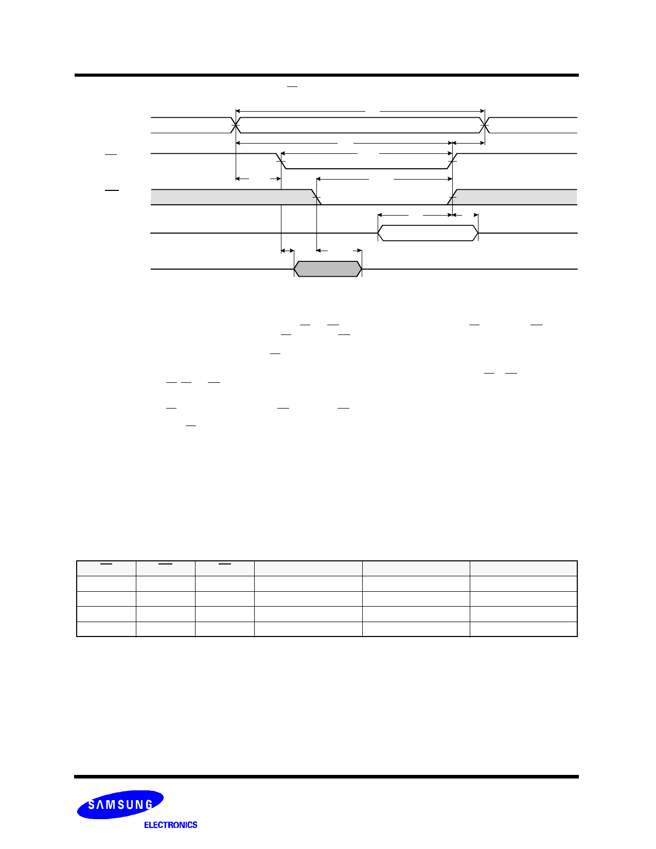
TIMING WAVEFORM OF WRITE CYCLE(3) (CS = Controlled)
Address
CS
tAS(4)
tWC
tAW
tCW(3)
tWP(2)
WE
Data in
Data out
High-Z
High-Z
tLZ
tWHZ(6)
tWR(5)
tDW
tDH
Data Valid
High-Z
High-Z(8)
NOTES(WRITE CYCLE)
1. All write cycle timing is referenced from the last valid address to the first transition address.
2. A write occurs during the overlap of a low CS and WE. A write begins at the latest transition CS going low and WE going low
A write ends at the earliest transition CS going high or WE going high. tWP is measured from the beginning of write to the end of
write.
3. tCW is measured from the later of CS going low to end of write.
4. tAS is measured from the address valid to the beginning of write.
5. tWR is measured from the end of write to the address change. tWR applied in case a write ends as CS or WE going high.
6. If OE, CS and WE are in the Read Mode during this period, the I/O pins are in the output low-Z state. Inputs of opposite phase
of the output must not be applied because bus contention can occur.
7. For common I/O applications, minimization or elimination of bus contention conditions is necessary during read and write cycle.
8. If CS goes low simultaneously with WE going or after WE going low, the outputs remain high impedance state.
9. Dout is the read data of the new address.
10. When CS is low : I/O pins are in the output state. The input signals in the opposite phase leading to the output should not be
applied.
FUNCTIONAL DESCRIPTION
CS
WE
OE
H
X
X*
L
H
H
L
H
L
L
L
X
* X means Don′t Care.
Mode
Not Select
Output Disable
Read
Write
I/O Pin
High-Z
High-Z
DOUT
DIN
Supply Current
ISB, ISB1
ICC
ICC
ICC
Rev 4.0
-7-
February 1998
Share Link: 