KM718V887 查看數據表(PDF) - Samsung
零件编号
产品描述 (功能)
生产厂家
KM718V887 Datasheet PDF : 16 Pages
| |||
KM718V887
256Kx18 Synchronous SRAM
256Kx18-Bit Synchronous Burst SRAM
FEATURES
• Synchronous Operation.
• On-Chip Address Counter.
• Write Self-Timed Cycle.
• On-Chip Address and Control Registers.
• VDD= 3.3V+0.3V/-0.165V Power Supply.
• VDDQ Supply Voltage 3.3V+0.3V/-0.165V for 3.3V I/O
or 2.5V+0.4V/-0.125V for 2.5V I/O.
• 5V Tolerant Inputs except I/O Pins.
• Byte Writable Function.
• Global Write Enable Controls a full bus-width write.
• Power Down State via ZZ Signal.
• Asynchronous Output Enable Control.
• ADSP, ADSC, ADV Burst Control Pins.
• LBO Pin allows a choice of either a interleaved burst or a
linear burst.
• Three Chip Enables for simple depth expansion with No Data
Contention.
• TTL-Level Three-State Output.
• 100-TQFP-1420A
FAST ACCESS TIMES
PARAMETER
Symbol -7 -8 -9 Unit
Cycle Time
tCYC 8.5 10 12 ns
Clock Access Time
tCD 7.5 8 9 ns
Output Enable Access Time tOE 3.5 3.5 3.5 ns
GENERAL DESCRIPTION
The KM718V887 is a 4,718,592 bit Synchronous Static Ran-
dom Access Memory designed for support zero wait state per-
formance for advanced Pentium/Power PC address pipelining.
And with CS1 high, ADSP is blocked to control signal.
It is organized as 256K words of 18 bits and integrates address
and control registers, a 2-bit burst address counter and high
output drive circuitry onto a single integrated circuit for reduced
components count implementation of high performance cache
RAM applications.
Write cycles are internally self-timed and synchronous.
The self-timed write feature eliminates complex off chip write
pulse shaping logic, simplifying the cache design and further
reducing the component count.
Burst cycle can be initiated with either the address status pro-
cessor(ADSP) or address status cache controller(ADSC)
inputs. Subsequent burst addresses are generated internally in
the system′s burst sequence and are controlled by the burst
address advance(ADV) input. ZZ pin controls Power Down
State and reduces Stand-by current regardless of CLK.
The KM718V887 is implemented in SAMSUNG′s high perfor-
mance CMOS technology and is available in a 100pin TQFP
package. Multiple power and ground pins are utilized to mini-
mize ground bounce.
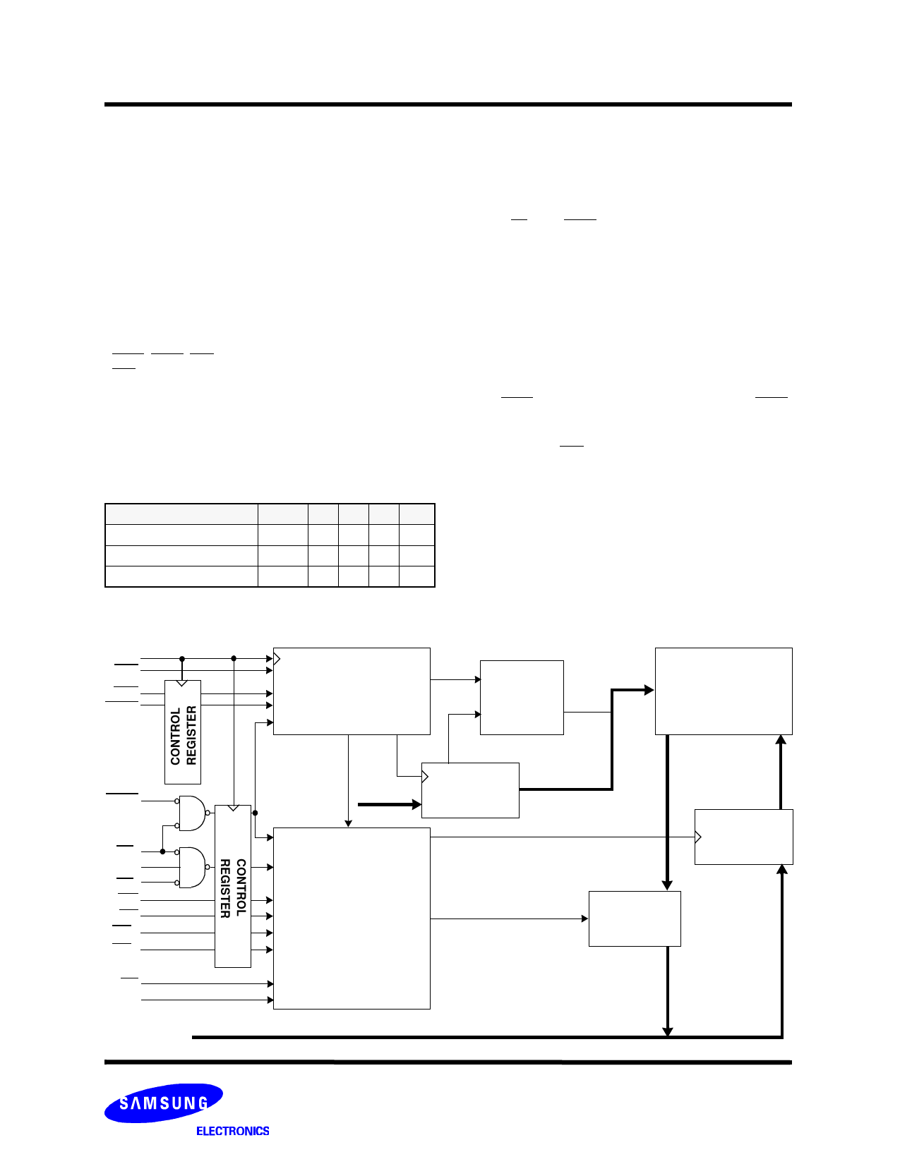
LOGIC BLOCK DIAGRAM
CLK
LBO
ADV
ADSC
BURST CONTROL
LOGIC
BURST
ADDRESS A′0~A′1
COUNTER
256Kx18
MEMORY
ARRAY
ADSP
CS1
CS2
CS2
GW
BW
WEa
WEb
OE
ZZ
DQa0 ~ DQb7
DQPa, DQPb
A0~A17
A0 ~ A1
ADDRESS
REGISTER
A2~A17
DATA-IN
REGISTER
CONTROL
LOGIC
OUTPUT
BUFFER
-2-
December 1998
Rev. 2.0
Share Link: 