KM718V887 查看數據表(PDF) - Samsung
零件编号
产品描述 (功能)
生产厂家
KM718V887 Datasheet PDF : 16 Pages
| |||
KM718V887
256Kx18 Synchronous SRAM
FUNCTION DESCRIPTION
The KM718V887 is a synchronous SRAM designed to support the burst address accessing sequence of the Pentium and Power PC
based microprocessor. All inputs(with the exception of OE, LBO and ZZ) are sampled on rising clock edges.
The start and duration of the burst access is controlled by ADSP, ADSC, ADV and Chip Select pins.
When ZZ is pulled HIGH, the SRAM will enter a Power Down State. At this time, internal state of the SRAM is preserved. When ZZ
returns to low, the SRAM normally operates after 2cycles of wake up time. ZZ pin is pulled down internally.
Read cycles are initiated with ADSP(or ADSC) using the new external address clocked into the on-chip address register when both
GW and BW are high or when BW is low and both WEa and WEb are high, When ADSP is sampled low, the chip selects are sampled
active, and the output buffer is enabled with OE, the data of cell array accessed by the current address are projected to the output
pins.
Write cycles are also initiated with ADSP(or ADSC)and are differentiated into two kinds of operations; All byte write operation and
individual byte write operation. All byte write occurs by enabling GW(in dependent of BW and WEx.), and individual byte write is per-
formed only when GW is High and BW is Low. WEa controls DQa0 ~ DQa7 and DQPa, WEb controls DQb0 ~ DQb7 and DQPb.
CS1 is used to enable the device and conditions internal use of ADSP and is sampled only when a new external address is loaded.
ADV is ignored at the clock edge when ADSP is asserted, but can be sampled on the subsequent clock edges. The address
increases internally for the next access of the burst when ADV is sampled low.
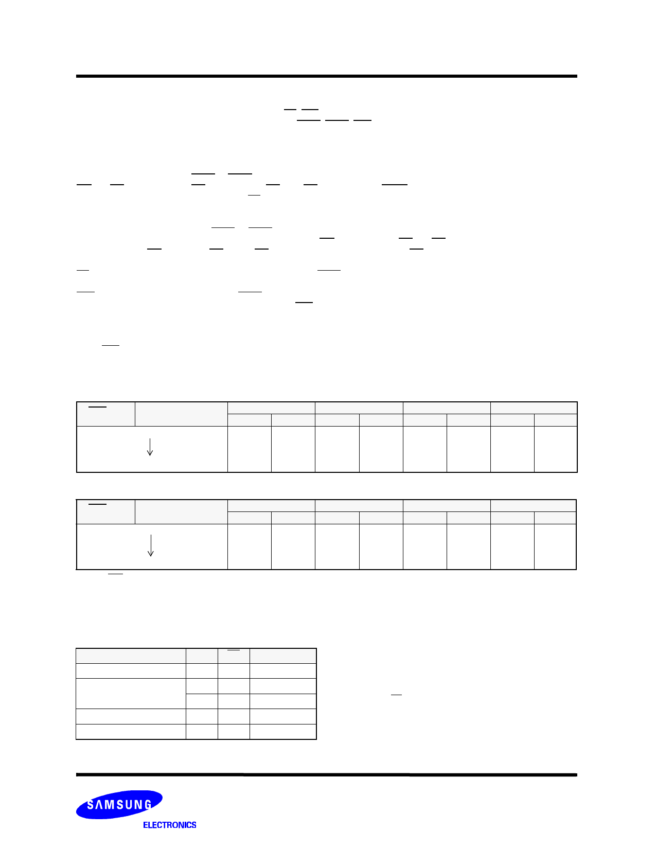
Addresses are generated for the burst access as shown below, The starting point of the burst sequence is provided by the external
address. The burst address counter wraps around to its initial state upon completion. The burst sequence is determined by the state
of the LBO pin. When this pin is low, linear burst sequence is selected. And when this pin is High, Interleaved burst sequence is
selected.
BURST SEQUENCE TABLE
LBO PIN
HIGH
First Address
Fourth Address
Case 1
A1
A0
0
0
0
1
1
0
1
1
Case 2
A1
A0
0
1
0
0
1
1
1
0
SEQUENCE TABLE
LBO PIN
LOW
First Address
Fourth Address
Case 1
A1
A0
0
0
0
1
1
0
1
1
Case 2
A1
A0
0
1
1
0
1
1
0
0
Note : 1. LBO pin must be tied to High or Low, and Floating State must not be allowed.
Case 3
A1
A0
1
0
1
1
0
0
0
1
Case 3
A1
A0
1
0
1
1
0
0
0
1
(Interleaved Burst)
Case 4
A1
A0
1
1
1
0
0
1
0
0
(Linear Burst)
Case 4
A1
A0
1
1
0
0
0
1
1
0
TRUTH TABLES
ASYNCHRONOUS TRUTH TABLE
(See Notes 1 and 2):
OPERATION
ZZ OE
Sleep Mode
H
X
Read
L
L
L
H
Write
L
X
Deselected
L
X
I/O STATUS
High-Z
DQ
High-Z
Din, High-Z
High-Z
Notes
1. X means "Don′t Care".
2. ZZ pin is pulled down internally
3. For write cycles that following read cycles, the output buffers must be
disabled with OE, otherwise data bus contention will occur.
4. Sleep Mode means power down state of which stand-by current does
not depend on cycle time.
5. Deselected means power down state of which stand-by current
depends on cycle time.
-4-
December 1998
Rev. 2.0
Share Link: 