KM718V887 查看數據表(PDF) - Samsung
零件编号
产品描述 (功能)
生产厂家
KM718V887 Datasheet PDF : 16 Pages
| |||
KM718V887
256Kx18 Synchronous SRAM
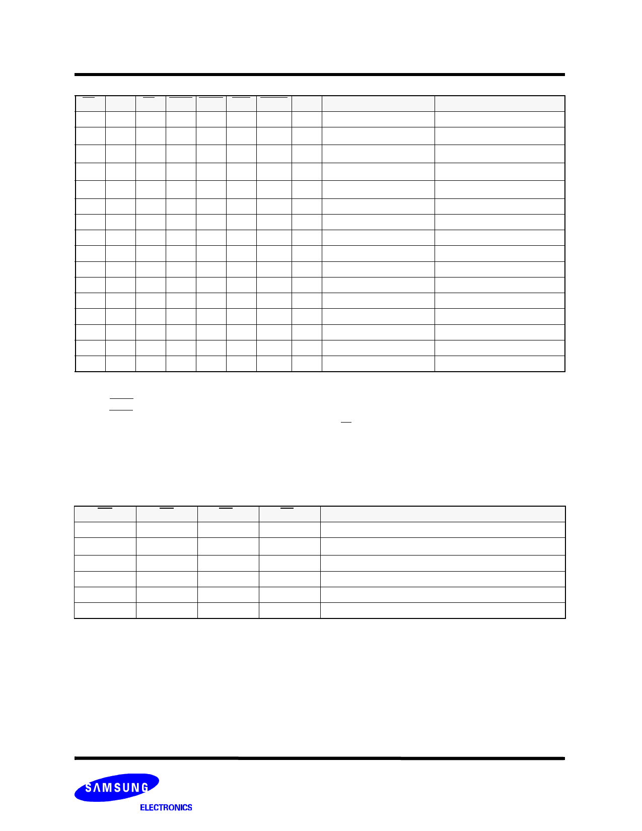
SYNCHRONOUS TRUTH TABLE
CS1 CS2 CS2 ADSP ADSC ADV WRITE CLK
H
X
X
X
L
X
X
↑
L
L
X
L
X
X
X
↑
ADDRESS ACCESSED
None
None
L
X
H
L
X
X
X
↑
None
L
L
X
X
L
X
X
↑
None
L
X
H
X
L
X
X
↑
None
L
H
L
L
X
X
X
↑
L
H
L
H
L
X
L
↑
L
H
L
H
L
X
H
↑
X
X
X
H
H
L
H
↑
H
X
X
X
H
L
H
↑
X
X
X
H
H
L
L
↑
H
X
X
X
H
L
L
↑
X
X
X
H
H
H
H
↑
H
X
X
X
H
H
H
↑
X
X
X
H
H
H
L
↑
H
X
X
X
H
H
L
↑
External Address
External Address
External Address
Next Address
Next Address
Next Address
Next Address
Current Address
Current Address
Current Address
Current Address
Notes : 1. X means "Don′t Care".
2. The rising edge of clock is symbolized by ↑.
3. WRITE = L means Write operation in WRITE TRUTH TABLE.
WRITE = H means Read operation in WRITE TRUTH TABLE.
4. Operation finally depends on status of asynchronous input pins(ZZ and OE).
OPERATION
Not Selected
Not Selected
Not Selected
Not Selected
Not Selected
Begin Burst Read Cycle
Begin Burst Write Cycle
Begin Burst Read Cycle
Continue Burst Read Cycle
Continue Burst Read Cycle
Continue Burst Write Cycle
Continue Burst Write Cycle
Suspend Burst Read Cycle
Suspend Burst Read Cycle
Suspend Burst Write Cycle
Suspend Burst Write Cycle
WRITE TRUTH TABLE
GW
BW
WEa
WEb
H
H
X
X
H
L
H
H
H
L
L
H
H
L
H
L
H
L
L
L
L
X
X
X
Notes : 1. X means "Don′t Care".
2. All inputs in this table must meet setup and hold time around the rising edge of CLK(↑).
OPERATION
READ
READ
WRITE BYTE a
WRITE BYTE b
WRITE ALL BYTEs
WRITE ALL BYTEs
-5-
December 1998
Rev. 2.0
Share Link: 