L6910(2003) 查看數據表(PDF) - STMicroelectronics
零件编号
产品描述 (功能)
生产厂家
L6910 Datasheet PDF : 21 Pages
| |||
L6910A L6910
Device Description
The device is an integrated circuit realized in BCD technology. The controller provides complete control logic and
protection for a high performance step-down DC-DC converter. It is designed to drive N Channel Mosfets in a
synchronous-rectified buck topology. The output voltage of the converter can be precisely regulated down to
900mV with a maximum tolerance of ±1.5% when the internal reference is used (simply connecting together
EAREF and VREF pins). The device allows also using an external reference (0.9V to 3V) for the regulation. The
device provides voltage-mode control with fast transient response. It includes a 200kHz free-running oscillator that
is adjustable from 50kHz to 1MHz. The error amplifier features a 10MHz gain-bandwidth product and 10V/µs slew
rate that permits to realize high converter bandwidth for fast transient performance. The PWM duty cycle can
range from 0% to 100%. The device protects against over-current conditions entering in HICCUP mode. The de-
vice monitors the current by using the rDS(ON) of the upper MOSFET(s) that eliminates the need for a current
sensing resistor. The device is available in SO16 narrow package.
Oscillator
The switching frequency is internally fixed to 200kHz. The internal oscillator generates the triangular waveform
for the PWM charging and discharging with a constant current an internal capacitor. The current delivered to the
oscillator is typically 50µA (Fsw = 200KHz) and may be varied using an external resistor (RT) connected between
OSC pin and GND or VCC. Since the OSC pin is maintained at fixed voltage (typ. 1.235V), the frequency is var-
ied proportionally to the current sunk (forced) from (into) the pin.
In particular connecting RT vs. GND the frequency is increased (current is sunk from the pin), according to the
following relationship:
fOSC,RT = 200KH z + -4--R-.-9--T--4-(---K-⋅---1Ω---0--)--6-
Connecting RT to VCC = 12V or to VCC = 5V the frequency is reduced (current is forced into the pin), according
to the following relationships:
fOSC,RT = 200KH z – -4---.R-3----T0---(6---K--⋅--Ω-1---0-)---7-
VCC = 12V
fOSC,RT = 200KH z – -R1---5-T---(-⋅--K-1---Ω-0---6-)-
VCC = 5V
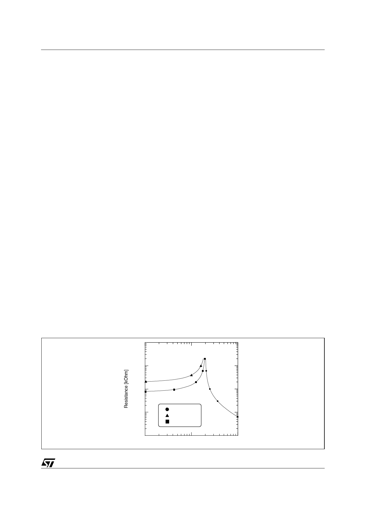
Switching frequency variation vs. RT are repeated in Fig. 1.
Note that forcing a 50µA current into this pin, the device stops switching because no current is delivered to the
oscillator.
Figure 1.
Reference
10000
1000
100
10
10
RT to GND
RT to VCC=12V
RT to VCC=5V
100
Frequency [kHz]
A precise ±1.5% 0.9V reference is available. This ref-
erence must be filtered with 1nF ceramic capacitor to
avoid instability in the internal linear regulator. It is
able to deliver up to 100µA and may be used as ref-
erence for the device regulation and also for other de-
vices. If forced under 70% of its nominal value, the
device enters in Hiccup mode until this condition is
removed.
Through the EAREF pin the reference for the regula-
tion is taken. This pin directly connects the non-in-
verting input of the error amplifier. An external
reference (or the internal 0.9V ±1.5%) may be used.
The input for this pin can range from 0.9V to 3V. It
has an internal pull-down (300kΩ resistor) that forces
the device shutdown if no reference is connected (pin
1000
floating). However the device is shut down if the volt-
age on the EAREF pin is lower than 650mV (typ).
5/21
Share Link: 