L6910(2003) 查看數據表(PDF) - STMicroelectronics
零件编号
产品描述 (功能)
生产厂家
L6910 Datasheet PDF : 21 Pages
| |||
L6910A L6910
Soft Start
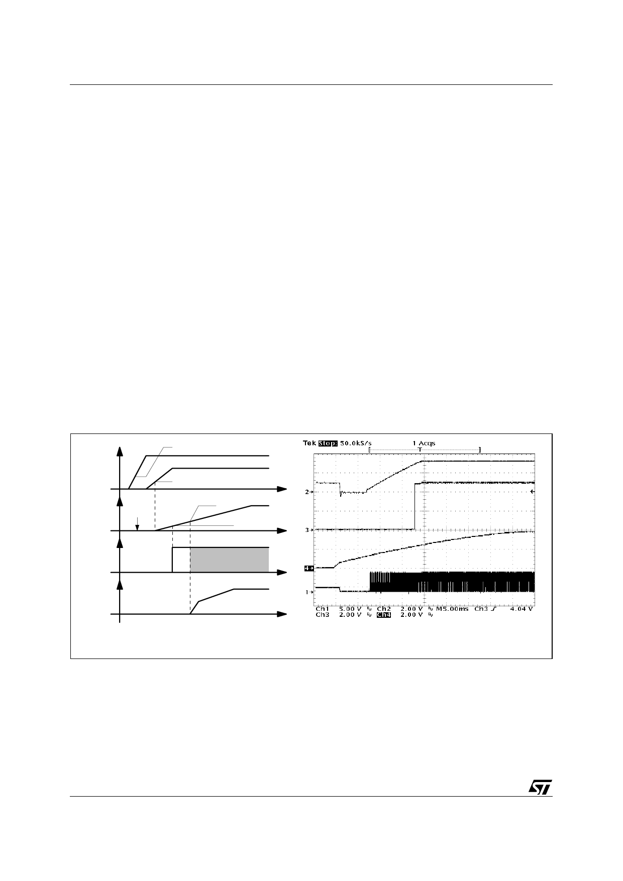
At start-up a ramp is generated charging the external capacitor CSS with an internal current generator. The initial
value for this current is of 35µA and speeds-up the charge of the capacitor up to 0.5V. After that it becames
10µA until the final charge value of approximatively 4V.
When the voltage across the soft start capacitor (VSS) reaches 0.5V the lower power MOS is turned on to dis-
charge the output capacitor. As VSS reaches 1.1V (i.e. the oscillator triangular wave inferior limit) also the upper
MOS begins to switch and the output voltage starts to increase.
No switching activity is observable if SS is kept lower than 0.5V and both mosfets are off.
If VCC and OCSET pins are not above their own turn-on thresholds and VEAREF is not above 650mV, the Soft-
Start will not take place, and the relative pin is internally shorted to GND. During normal operation, if any under-
voltage is detected on one of the two supplies, the SS pin is internally shorted to GND and so the SS capacitor
is rapidly discharged.
Figure 2. Soft Start (with Reference Present)
Vcc
Vin
Vcc Turn-on threshold
Vin Turn-on threshold
Vss
to GND
1V
0.5V
LGATE
Vout
Timing Diagram
Acquisition: CH1 = PHASE; CH2 = Vout;
CH3 = PGOOD; CH4 = Vss
Driver Section
The driver capability on the high and low side drivers allows using different types of power MOS (also multiple
MOS to reduce the RDSON), maintaining fast switching transition.
The low-side mos driver is supplied directly by Vcc while the high-side driver is supplied by the BOOT pin.
Adaptative dead time control is implemented to prevent cross-conduction and allow to use several kinds of mos-
fets. The upper mos turn-on is avoided if the lower gate is over about 200mV while the lower mos turn-on is
avoided if the PHASE pin is over about 500mV. The lower mos is in any case turned-on after 200ns from the
high side turn-off.
The peak current is shown for both the upper (fig. 3) and the lower (fig. 4) driver at 5V and 12V. A 3.3nF capac-
itive load has been used in these measurements.
For the lower driver, the source peak current is 1.1A @ VCC = 12V and 500mA @ VCC = 5V, and the sink peak
current is 1.3A @ VCC = 12V and 500mA @ VCC = 5V.
Similarly, for the upper driver, the source peak current is 1.3A @ Vboot-Vphase = 12V and 600mA @ Vboot-
Vphase = 5V, and the sink peak current is 1.3A @ Vboot-Vphase =12V and 550mA @ Vboot-Vphase = 5V.
6/21
Share Link: 