L6926Q1(2008) 查看數據表(PDF) - STMicroelectronics
零件编号
产品描述 (功能)
生产厂家
L6926Q1 Datasheet PDF : 16 Pages
| |||
L6926
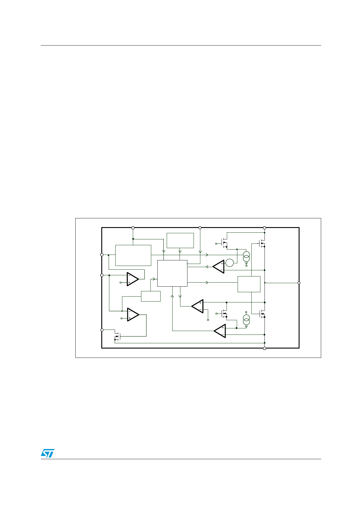
4
Operation description
Operation description
The main loop uses slope compensated PWM current mode architecture. Each cycle the
high side MOSFET is turned on, triggered by the oscillator, so that the current flowing
through it (the same as the inductor current) increases. When this current reaches the
threshold (set by the output of the error amplifier E/A), the peak current limit comparator
PEAK_CL turns off the high side MOSFET and turns on the low side one until the next clock
cycle begins or the current flowing through it goes down to zero (ZERO CROSSING
comparator). The peak inductor current required to trigger PEAK_CL depends on the slope
compensation signal and on the output of the error amplifier.
In particular, the error amplifier output depends on the VFB pin voltage. When the output
current increases, the output capacitor is discharged and so the VFB pin decreases. This
produces increase of the error amplifier output, so allowing a higher value for the peak
inductor current. For the same reason, when due to a load transient the output current
decreases, the error amplifier output goes low, so reducing the peak inductor current to
meet the new load requirements.
The slope compensation signal allows the loop stability also in high duty cycle conditions
(see related section)
Figure 2. Device block diagram
SYNC
RUN
VCC
COM P
LOW
NOISE/
CONSUM PTION
OSCILLATOR
GND
SENSE
PMOS
SLOP E
POWER
PMOS
GND
LOOP
PEAK
FB
E/A
CONTROL
CL
VREF
DRIVER
LX
0.6V
OVP
PGOOD
VREF
0.9V
PGOOD
ZERO
Vcc
CROSSING
GND
SENSE Vcc
NMOS
VALLEY
CL
POWER
NMOS
GND
7/16
Share Link: 