L6932(2003) 查看數據表(PDF) - STMicroelectronics
零件编号
产品描述 (功能)
生产厂家
L6932 Datasheet PDF : 10 Pages
| |||
L6932
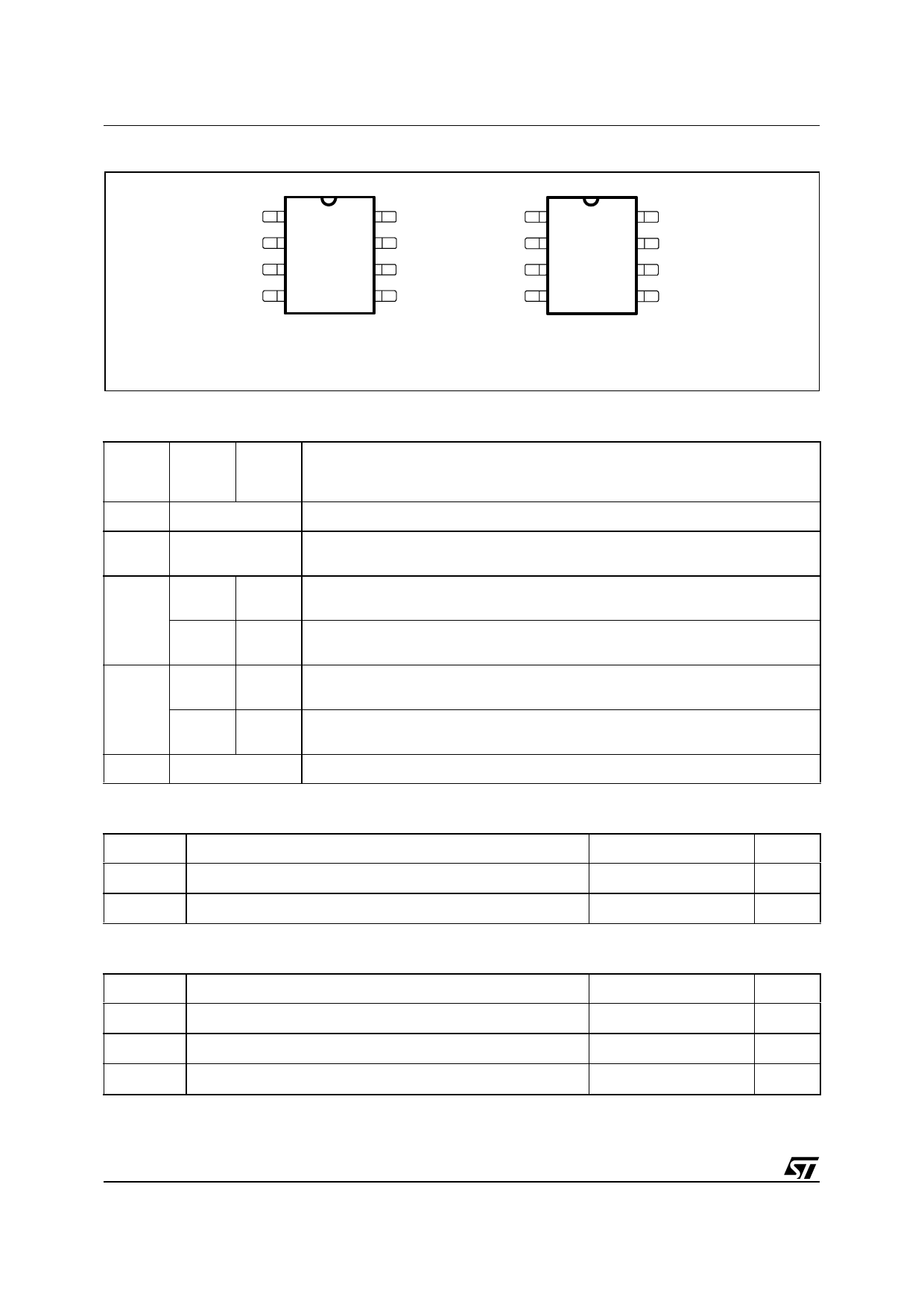
PIN CONNECTIONS
EN
IN
ADJ
OUT
1
8
2
7
3
6
4
5
L6932D1.2
GND
GND
GND
GND
EN
IN
OUT
PGOOD
1
8
2
7
3
6
4
5
L6932D1.8
L6932D2.5
GND
GND
GND
GND
PIN FUNCTION
N°
L6232D L6232D
1.2
1.8/2.5
Description
1
EN
Enables the device if connected to Vin and disables the device if forced to gnd.
2
IN
Supply voltage. This pin is connected to the drain of the internal N-mos. Connect this
pin to a capacitor larger than 10µF.
ADJ
–
Connecting this pin to a voltage divider it is possible to programme the output voltage
between 1.2V and 5V.
3
–
OUT Regulated output voltage. This pin is connected to the source of the internal N-mos.
Connect this pin to a capacitor of 10µF.
OUT
–
Regulated output voltage. This pin is connected to the source of the internal N-mos.
Connect this pin to a capacitor of 10µF.
4
–
PGOOD Power good output. The pin is open drain and detects the output voltage. It is forced
low if the output voltage is lower than 90% of the programmed voltage.
5, 6, 7, 8
GND
Ground pin.
ABSOLUTE MAXIMUM RATINGS
Symbol
Vin
VIN and Pgood
EN, OUT and ADJ
Parameter
Value
14.5
-0.3 to (Vin +0.3)
Unit
V
V
THERMAL DATA
Symbol
Parameter
Rth J-amb Thermal Resistance Junction to Ambient
Tmax
Maximum Junction Temperature
Tstg
Storage Temperature Range
(*) Measured on Demoboard with about 4 cm2 of dissipating area 2 Oz.
Value
62 (*)
150
-65 to 150
Unit
°C/W
°C
°C
2/10
Share Link: 