LB11872H(2002) 查看數據表(PDF) - SANYO -> Panasonic
零件编号
产品描述 (功能)
生产厂家
LB11872H Datasheet PDF : 13 Pages
| |||
Continued from preceding page.
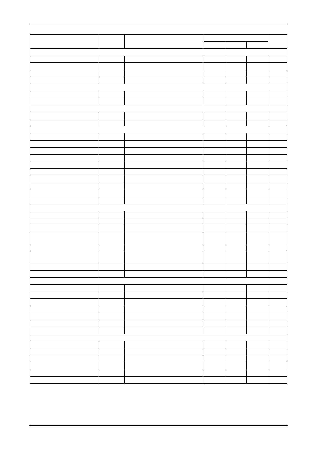
LB11872H
Parameter
[Lock Detection Output]
Output saturation voltage
Output leakage current
[FG Output]
Output saturation voltage
Output leakage current
[Drive Block]
Dead zone width
Output idling voltage
Forward gain 1
Forward gain 2
Reverse gain 1
Reverse gain 2
Acceleration command voltage
Deceleration command voltage
Forward limiter voltage
Reverse limiter voltage
[CSD Oscillator Circuit]
Oscillation frequency
High-level pin voltage
Low-level pin voltage
External capacitor charge and discharge current
Lock detection delay count
Clock cutoff protection operating count
Lock protection count
Initial reset voltage
[Clock Input Block]
External input frequency
High-level input voltage
Low-level input voltage
Input open voltage
Hysteresis width
High-level input current
Low-level input current
[S/S Pin]
High-level input voltage
Low-level input voltage
Input open voltage
Hysteresis width
High-level input current
Low-level input current
Symbol
Conditions
VLD (SAT) ILD = 10 mA
ILD (LEAK) VLD = 28 V
VFG (SAT) IFG = 5 mA
IFG (LEAK) VFG = 28 V
VDZ
VID
GDF+1
GDF+2
GDF–1
GDF–2
VSTA
VSTO
VL1
VL2
With the phase is locked
With phase locked
With phase unlocked
With phase locked
With phase unlocked
Rf = 22 Ω
Rf = 22 Ω
fOSC
VCSDH
VCSDL
ICHG
CSDCT1
C = 0.022 µF
CSDCT2
CSDCT3
VRES
fCLK
VIH (CLK) Design target value
VIL (CLK) Design target value
VIO (CLK)
VIS (CLK) Design target value
IIH (CLK) V (CLK) = VREG
IIL (CLK) V (CLK) = 0 V
VIH (S/S)
VIL (S/S)
VIO (S/S)
VIS (S/S)
IIH (S/S)
IIL (S/S)
V (S/S) = VREG
V (S/S) = 0 V
Ratings
Unit
min
typ
max
0.15
0.5
V
10
µA
0.15
0.5
V
10
µA
50
100
300 mV
6 mV
0.4
0.5
0.6 deg
0.8
1.0
1.2 deg
–0.6
–0.5
–0.4 deg
–0.8
–1.0
–1.2 deg
5.0
5.6
V
0.8
1.5
V
0.53
0.59
0.65
V
0.32
0.37
0.42
V
31
Hz
4.3
4.8
5.3
V
0.75
1.15
1.55
V
3
5
7
µA
7
2
31
0.60
0.80
V
400
2.0
0
2.7
0.1
–185
3.0
0.2
140
–140
10000
Hz
VREG
V
1.0
V
3.3
V
0.3
V
185
µA
µA
2.0
0
2.7
0.1
–185
3.0
0.2
140
–140
VREG
V
1.0
V
3.3
V
0.3
V
185
µA
µA
Three-Phase Logic
IN1
IN2
IN3
H
L
H
H
L
L
H
H
L
L
H
L
L
H
H
L
L
H
OUT1 to OUT3 (H: Source, L: Sink)
OUT1
L
L
M
H
H
M
OUT2
H
M
L
L
M
H
OUT3
M
H
H
M
L
L
For IN1 to IN3, “H” means that IN+ is greater than IN–, and “L” means IN– is greater than IN+.
For OUT1 to OUT3, “H” means the output is a source, and “L” means that it is a sink.
No. 7257 -3/13
Share Link: 