LB1857 查看數據表(PDF) - SANYO -> Panasonic
零件编号
产品描述 (功能)
生产厂家
LB1857 Datasheet PDF : 6 Pages
| |||
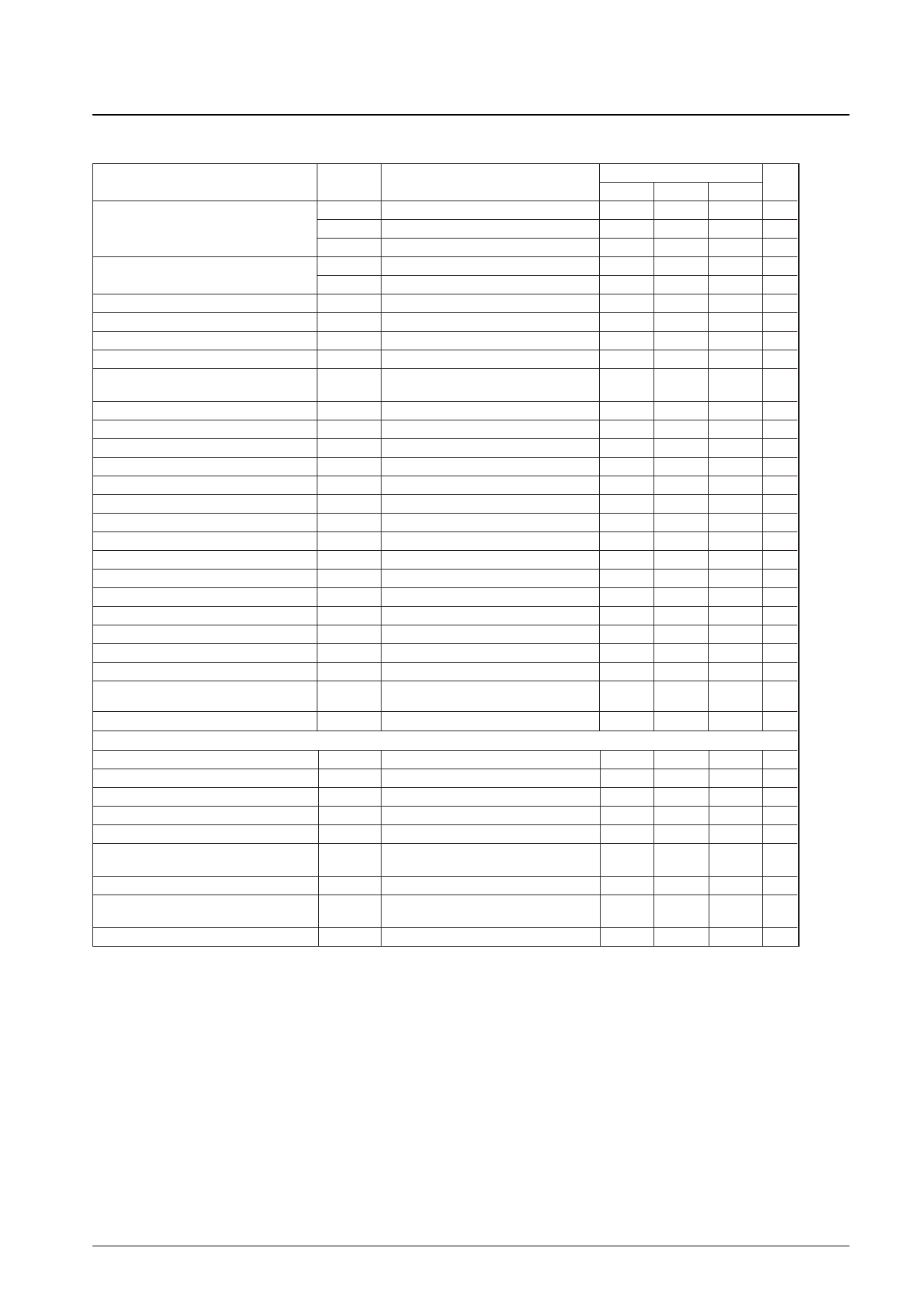
LB1857M
Electrical Characteristics at Ta = 25°C, VCC1 = 5 V, VCC2 = 7 V, VS = 3 V
Parameter
Supply current
Output quiescent current
Output saturation voltage
Output TRS withstand voltage
Output quiescent voltage
Hall amplifier input offset voltage
Hall amplifier common mode input
voltage range
Hall I/O voltage gain
Brake pin high level voltage
Brake pin low level voltage
Brake pin input current
Brake pin leakage current
FRC pin high level voltage
FRC pin low level voltage
FRC pin input current
FRC pin leakage current
Upper side residual voltage
Lower side residual voltage
Overlap level
Standby on voltage
Standby off voltage
Standby pin bias current
Thermal protection circuit operating
temperature
Thermal protection circuit hysteresis
[FG amplifier]
Input offset voltage
Open loop voltage gain
Source output saturation voltage
Sink output saturation voltage
Common mode signal exclusion ratio
FG amplifier common mode input
voltage range
Phase margin
Schmitt amplifier threshold voltage
Schmitt amplifier hysteresis width
Symbol
ICC1
ICC2
IS
ICCOQ
ISOQ
VO(sat)
VO(sus)
VOQ
VHOFFSET
VHCOM
GVHO
VBRH
VBRL
IBRIN
IBRLEAK
VFRCH
VFRCL
IFRCIN
IFRCLEAK
VXH
VXL
OL
VSTBYL
VSTBYH
ISTBYIN
TTSD
∆TTSD
Conditions
VBR = 5 V
VBR = 5 V
VBR = 5 V, RL = ∞
VSTBY = 0 V
VSTBY = 0 V, RL = ∞
IOUT = 0.6 A, sink + source
IOUT = 20 mA*1
VBR = 5 V
*1
Rangle = 8.2 kΩ
IOUT = 100 mA, VCC2 = 6 V, VS = 2 V
IOUT = 100 mA, VCC2 = 6 V, VS = 2 V
VCC2 = 6 V, VS = 3 V
*2
*1
*1
VFG OFFSET
GVFG
VFG OU
VFG OD
CHR
f = 1 kHz
IO = –2 mA
IO = 2 mA
*1
VFG CH
φM
VFGS SH
VFGS HIS
*1
VFGIN+ = 2.5 V,
when VFGOUT2 goes from high to low
VFGIN+ = 2.5 V
min
16
1.4
–5
1.4
32.0
2.0
2.8
0.32
0.39
60
–0.2
2
150
–8
3.7
0
2.45
20
Ratings
typ
4.5
13
6.5
1.5
35.0
70
180
15
60
80
20
2.50
40
Note: 1. These are target settings, and are not measured. The overlap ratings are taken as test ratings without change.
2. When the standby pin is open the IC will be in the standby state.
Unit
max
6.5 mA
20 mA
9.0 mA
180 µA
150 µA
2.3 V
V
1.6 V
+5 mV
2.8 V
38.0 dB
V
0.8 V
100 µA
–30 µA
V
1.2 V
100 µA
–30 µA
0.49 V
0.48 V
80 %
+0.1 V
5V
10 µA
210 °C
°C
+8 mV
dB
V
1.3 V
dB
3.5 V
deg
2.55 V
60 mV
No. 3976-2/6
Share Link: 