LB1862(1999) 查看數據表(PDF) - SANYO -> Panasonic
零件编号
产品描述 (功能)
生产厂家
LB1862 Datasheet PDF : 7 Pages
| |||
LB1862
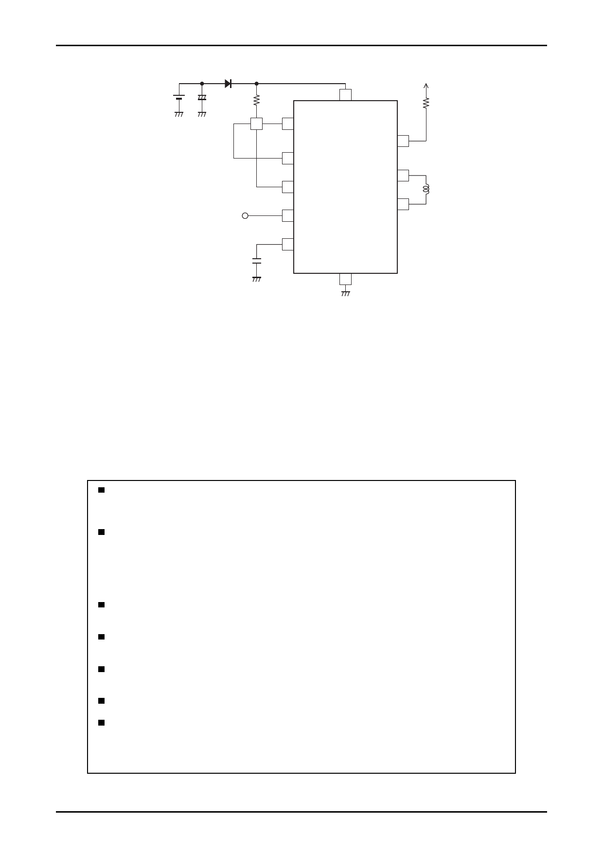
Design reference
(1) VCC pin
Power supply pin for control block and motor drive.
Accepts a wide operation voltage range from 3.8 to 16.8V, for 5V/12V dual power supply support.
(2) OUT1, OUT2 pins
Single-phase coil output pins.
Bipolar drive output with upper side inverted and lower side single output. Built-in regenerative circuit regenerates
kickback current between lower side NPN outputs when a diode is used for protection against IC destruction caused
by reverse connection.
(3) IN–, IN+ pins
Hall input signal pins
The Hall signal is amplified into a square wave by the Hall amplifier with hysteresis characteristics of ±3.5 mV
(typ.). The Hall input signal amplitude should be 70 mV or more.
(4) CT pin
This pin serves for connecting a capacitor between CT and GND.
The capacitor determines the characteristics of the built-in lockup protection circuit for preventing coil burnout in
the case of motor restraint. Once normal motor load is restored, the automatic recovery circuit resets itself.
Changing the capacitance alters the lockup detection time.
When a 0.47 µF capacitor is connected between CT and GND
Lockup detection time
: approx. 0.5s
Lockup protection time/automatic recovery time : approx. 0.16s (output ON)
approx. 1s (output OFF)
When not using lockup protection function, this pin should be connected to ground.
(5) RD pin
Open-collector output pin that is Low during rotation and OFF when lockup is detected.
The output is a latch type which stays OFF also when the automatic recovery circuit has restored drive mode, unless
the rotation actually resumes.
(6) ST pin and HB pin
ST pin : When input to this pin is High, motor drive is stopped (OUT is high impedance).
At this time, RD output indicates lockup protection mode OFF.
HB pin : Hall bias switching pin. At ST pin High input, Hall bias is cut off to reduce current drain in fan standby
mode.
If not used, both pins should be open.
(7) Thermal protection circuit
When internal temperature Tj of IC reaches 180°C, output current limiter is activated to protect against damage.
No. 6208-6/7
Share Link: 