LC72709E 查看數據表(PDF) - SANYO -> Panasonic
零件编号
产品描述 (功能)
生产厂家
LC72709E Datasheet PDF : 16 Pages
| |||
LC72709E, 72709W
Operation During Reset and in Standby Mode
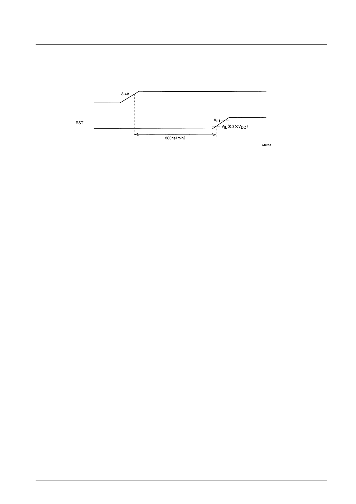
• The Reset Signal
A reset operation is performed by holding the RST pin input level under VIL for at least 300 ns when the power-supply
voltage (VDD) is over 3.4 V. (See the figure below.) Applications must apply a reset when power is first applied or
when power is reapplied.
VDD voltage
• Pin Outputs During a Reset (LC72709E)
Low-level outputs: CLK16 (7), DATA (8), FCK (20), BCK (21), FLOCK (22), BLOCK (25), CRC4 (26), IC1 (3), IC2 (4)
High-level outputs: INT (27), XOUT (1)
Open: DO (31)
• Pin Outputs During a Reset (LC72709W)
Low-level outputs: CLK16 (10), DATA (11), FCK (28), BCK (30), FLOCK (31), BLOCK (36), CRC4 (38), IC1 (4),
IC2 (6)
High-level outputs: INT (39), XOUT (2)
Open: DO (45)
• Reset Operating Range
The output pin states according to the reset signal are stipulated by item “Pin outputs during a reset” above. The IC
internal flip-flops are all reset. Although the delay shift registers are also reset, the memory array is not influenced.
However, since memory refresh operation stops, data cannot be retained. The crystal oscillator circuit does not stop.
• Data Input After a Reset
After a reset completes and at least one full clock cycle (about 278 ns at 3.6 MHz, this is the IC’s main clock) has
elapsed, the serial input control circuit will be able to operate and accept data.
• Standby Mode
The IC can be set to standby mode by setting the STNBY pin high. Since all IC operations are stopped in this mode,
this produces a state essentially equivalent to the power off state. (Note that after standby mode has been cleared, a wait
period is required until the crystal oscillator circuit is operating stably.) The pin output states in standby mode are
identical to the states after a reset as described in item “Pin outputs during a reset” above.
Notes on Post Error Correction Output Data
• The received data is error corrected using (272, 190) codes in single block (272 bits) units. An error check using the
layer 2 CRC is also performed. After error correction, the IC prepares for transfer of the data to the CPU and outputs
the INT signal. This is referred to as horizontal correction output.
• However, the INT signal is not output at this time if the corresponding output data does not meet all of the following
three conditions.
— Error correction completed and it passed the layer 2 CRC check.
— The data was received while both block and frame synchronization were established.
— The data was packet data.
Note that all received packet data can be acquired by setting bit 5 (INT) in the control register.
• If the data could not be corrected by the horizontal correction system, correction using product codes is performed in frame
units. This is called vertical correction. The data that can be acquired at the output of the vertical correction is the following.
— Data that was fully corrected in horizontal correction is not output.
— Packet data that could not be corrected by horizontal correction but that was fully corrected by vertical correction is output.
— Packet data that could not be corrected by either horizontal or vertical correction is not output.
Note that, as is the case for horizontal correction output, all received packet data can be acquired by setting bit 5 (INT) in the
control register. However, the parity packet data corrected by vertical correction cannot be output even if this flag bit is set.
No. 5876-10/16
Share Link: 