LC72709E 查看數據表(PDF) - SANYO -> Panasonic
零件编号
产品描述 (功能)
生产厂家
LC72709E Datasheet PDF : 16 Pages
| |||
LC72709E, 72709W
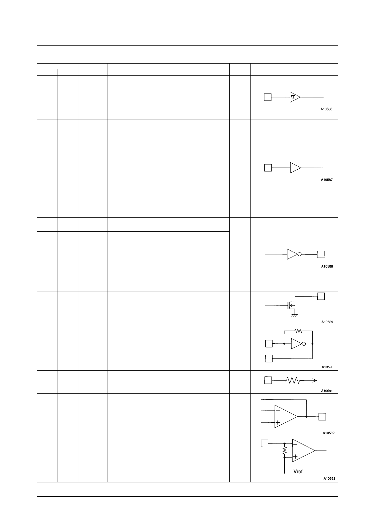
Pin Descriptions
Pin No.
LC72709E LC72709W
28
40
29
42
30
43
33
47
32
46
40
58
9
13
12
18
13
19
14
20
15
22
16
23
17
24
18
26
19
27
41
59
42
61
5
7
6
9
7
10
8
11
20
29
21
30
22
31
25
36
26
38
27
39
3
5
4
6
Pin Name
CL
CE
DI
RST
STNBY
TEST
TP0
TP1
TP2
TP3
TP4
TP5
TP6
TP7
TP8
TPC1
TPC2
TOSEL1
TOSEL2
CLK16
DATA
FCK
BCK
FLOCK
BLOCK
CRC4
INT
IC1
IC2
Function
CCB serial interface
Clock input
Data control input
Data input
System reset input (active low)
Standby mode (active high)
Test (Must be connected to ground during normal operation.)
Must be connected to either VDD or VSS.
Clock regeneration monitor
Demodulated data monitor
Frame start signal output
Block start signal output
Outputs a high level during frame synchronization.
Outputs a high level during block synchronization.
Layer 4 CRCC check result output
External CPU interrupt signal
Internal connections. These pins must be left open.
I/O
Input
Input
Output
31
44
DO
Data output used by the CCB serial interface
Output
44
63
XIN
System clock generation crystal oscillator element Input
1
2
XOUT connections
Output
36
52
MPXIN Baseband (multiplex) signal input
Input
38
55
FLOUT Subcarrier output (76-kHz filter output)
Output
Circuit type
39
57
CIN
Subcarrier input (comparator input)
Input
Continued on next page.
No. 5876-4/16
Share Link: 