LC72709E 查看數據表(PDF) - SANYO -> Panasonic
零件编号
产品描述 (功能)
生产厂家
LC72709E Datasheet PDF : 16 Pages
| |||
Continued from preceding page.
Pin No.
LC72709E LC72709W Pin Name
LC72709E, 72709W
Function
I/O
35
51
VREF
Reference voltage output (Vdda/2)
Output
Circuit type
37
54
VDDA
Analog system power supply
—
34
50
VSSA
Analog system ground
—
2, 10, 24 3, 14, 35, VDDD
Digital system power supply (4.5 to 5.5 V)
—
11,23, 43 15, 34, 62 VSSD
Digital system ground
—
1, 4, 8,
12, 16,
17, 21,
25, 28,
–
32, 33,
37, 41,
45, 48,
49, 53,
56, 60,
64
NC
Not connection
Note: A capacitor of at least 2000 pF must be inserted between VDDD and VSSD when using this IC.
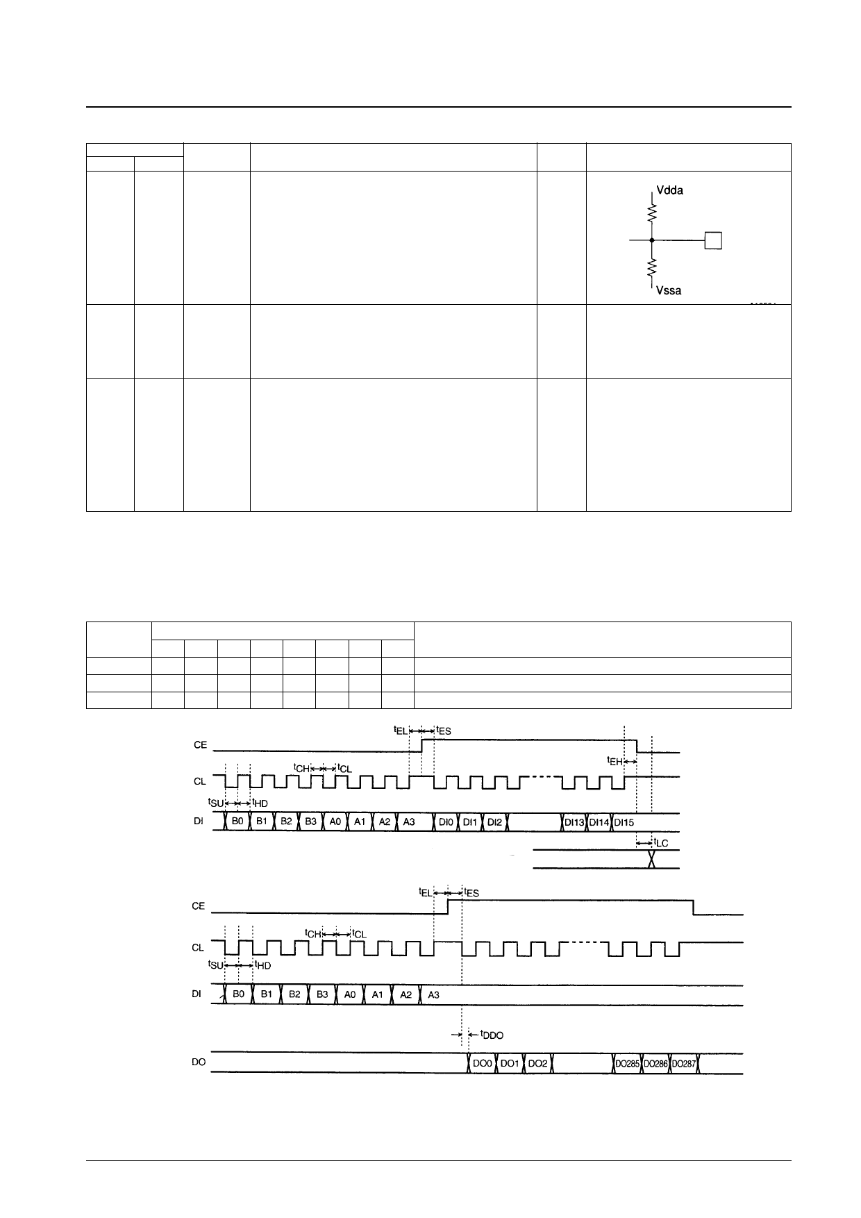
Data I/O Techniques
• CCB Technique
Sanyo audio ICs input and output data using the Sanyo CCB (computer control bus) standard, which is a serial bus
format. This IC uses an 8-bit address CCB and uses the following addresses.
Address
I/O mode
B0 B1 B2 B3 A0 A1 A2 A3
Function
Input
0
1
0
1
1
1
1
1 16-bit control data input
Output
1
1
0
1
1
1
1
1 Data output for the input clock (CL)
Input
0
0
1
1
1
1
1
1 Data input (in 8-bit units) for the layer 4 CRC check circuit
• Data Input Timing
• Data Output Timing
Internal data latching
A10595
A10596
Note:The DO pin is normally left open.
Since the DO pin is an n-channel open drain pin, the time required for the data to change from the low level to the high level depends on the value of
the pull-up resistor.
No. 5876-5/16
Share Link: 