LC72714 查看數據表(PDF) - SANYO -> Panasonic
零件编号
产品描述 (功能)
生产厂家
LC72714 Datasheet PDF : 29 Pages
| |||
LC72714W
Frame Synchronization: Error Protection Count
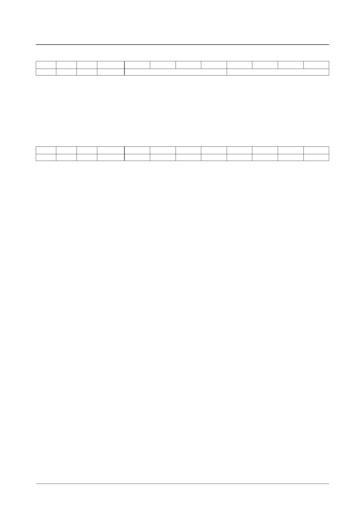
Address Register R/W Initial value
03H SYNCF
W
17H
BIT7
BIT6
BIT5
Back protection
BIT4
(LSB)
BIT3
BIT2
BIT1
Forward protection
BIT0
(LSB)
This IC detects the BIC characteristic inflection points which occur at four places in a single frame, and increments or
decrements a protection counter depending on whether or not they match the IC internal frame synchronization timing
counter.
As is the case with the block synchronization error protection value, applications must set these to values one less than
the desired protection count. The default values are 8 for the frame synchronization forward protection count and 2 for
the back protection count.
Control Register 1
Address Register R/W
04H
CTL1
W
*: BIT0 and BIT1 are unused.
Initial value
BIT7
BIT6
BIT5
BIT4
BIT3
BIT2
00H
CRC4_RST DO_MOVE INT_MOVE SYNC_RST EC_STOP VEC_HALT
BIT1
*
BIT0
*
• VEC_HALT
0: Vertical correction and the second horizontal correction processing are performed. (default)
1: Vertical correction and the second horizontal correction processing are not performed.
All IC operations related to vertical correction and the second horizontal correction are stopped by setting this flag.
Note that in data output, only data to which the first horizontal correction has been applied will be output.
• EC_STOP
0: All functions operate. (default)
1: Only the MSK detection circuit and the synchronization regeneration circuit operate.
This flag stops all operations relating to error correction (including RAM access), data output, and other operations.
While all IC operations are stopped in standby mode, MSK demodulation, the synchronization circuit, the serial data
input circuit, and the layer 4 CRC circuit continue to operate in this mode.
• SYNC_RST
0: (default)
1: Resets just the synchronization regeneration circuit.
Clears the synchronization status and the synchronization protection status in the synchronization circuit block, and
sets the circuit to the unsynchronized state. This allows the circuit to quickly pull in to frame synchronization when
the frame synchronization is incorrect for the new reception data following tuning, when the radio has been tuned to
a new station. While this flag is used for synchronization related sections of the system, it does not initialize the
registers that set the number of allowable BIC errors, the block synchronization forward and back protection counts,
and the frame synchronization forward and back protection counts. Also note that during a synchronization block
reset, the INT signal is not output and the DO pin outputs a high level (high-impedance).
This flag is not automatically reset to 0. Applications must send a 0 value after setting this flag.
• INT_MOVE
0: Data is only output when error correction has completed, layer 2 CRC has completed, and the data was received with
the circuit synchronized. (default)
1: All data is output. (Operation is identical to that of the LC72700E.)
In the default state, this IC only outputs data that has been fully error corrected and that was received in both block
and frame synchronization. (This also includes the layer 2 CRC check.)
To acquire all data as provided by the LC72700, applications must set both this flag and the VEC_OUT (BIT2) flag
in control register 2 as described below.
• DO_MOVE (Valid only when SP is high.)
0: The high state (high impedance) is held at all times other than when data is being output. (default)
1: Operate identically to the LC72700 when changes are linked to the INT signal, i.e. when both INT_MOVE and
VEC_OUT are set to 1.
• CRC4_RST
0: (default)
1:Reset the layer 4 CRC detection circuit.
This flag is not automatically reset to 0. Applications must send a 0 value after setting this flag.
No. 6871-8/29
Share Link: 