LC72714 查看數據表(PDF) - SANYO -> Panasonic
零件编号
产品描述 (功能)
生产厂家
LC72714 Datasheet PDF : 29 Pages
| |||
LC72714W
Control Register 2
Address Register R/W Initial value
BIT7
BIT6
BIT5
BIT4
BIT3
BIT2
BIT1
BIT0
05H
CTL2
W
00H
SUBBLK BLK_RST DACK
DREQ
RDY
VEC_OUT DMA_RD
DMA
• DMA (Valid only when SP is low.)
0: Do not use DMA transfer for readout of post-error correction data. (default)
1: Use DMA transfer for readout of post-error correction data.
• DMA_RD (Valid only when SP is low.)
0: Use the RD signal as the DMA transfer read control signal. (default)
1: Use the DACK signal as the DMA transfer read control signal.
• VEC_OUT
0: Do not perform post-horizontal correction output when vertical correction processing is not performed. (default)
1: Output all data, even when vertical correction processing is not performed. (Operation identical to that of the
LC72700)
When this flag is set and a frame of data with absolutely no errors is received, data that is completely identical to the
corresponding post-horizontal correction data is output with the timing of the output of post-vertical correction data,
even if vertical correction is not performed.
This flag must be set to create interface specifications identical to those of the LC72700.
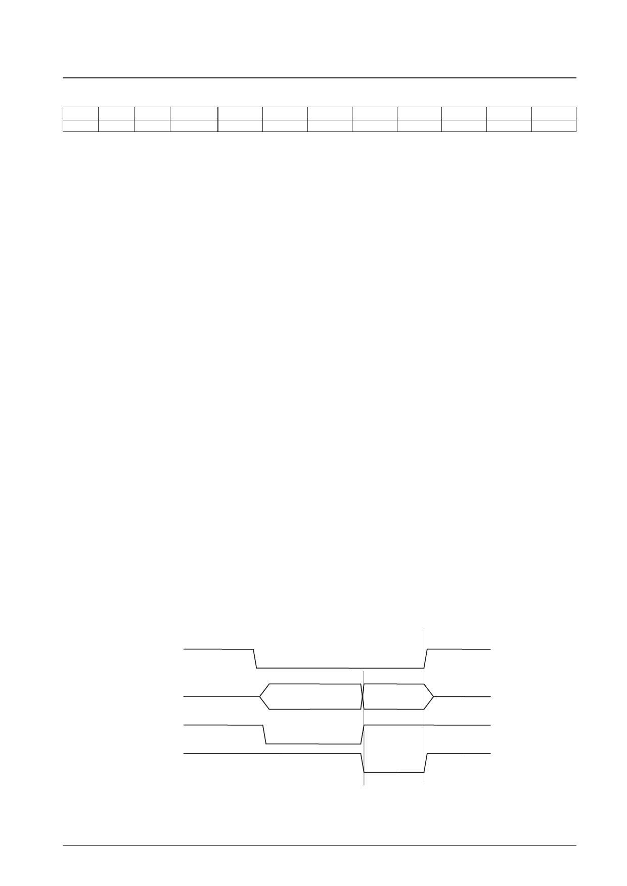
• RDY (Valid only when SP is low.)
0: The RDY output is issued with timing 1. (default)
1: The RDY output is issued with timing 2.
• DREQ (Valid only when SP is low.)
0: Negative logic is used for the polarity of the DREQ signal. (default)
1: Positive logic is used for the polarity of the DREQ signal.
• DACK (Valid only when SP is low.)
0: Negative logic is used for the polarity of the DACK signal. (default)
1: Positive logic is used for the polarity of the DACK signal.
• BLK_RST
0: (default)
1: Resets the block synchronization circuit only.
Sets the block synchronization status to unsynchronized and clears the block synchronization protection counter.
However, note that this has no effect on the frame synchronization functions. Also note that during a
synchronization block reset, the INT signal is not output and the DO pin outputs a high level (high-impedance).
This flag is not automatically reset to 0. Applications must send a 0 value after setting this flag.
• SUBBLK
0: Normal status. (default)
1: Set to 1 when a substation (for example a dGPS station during VICS reception) is temporarily received.
The SUBBLK and BLK_RST flags are mainly used when receiving and processing VICS data and dGPS data at the
same time. (See page 28.)
RD
DATn
RDY
Timing1
RDY
Timing2
Valid
output
RDY Signal Output Timing
No. 6871-9/29
Share Link: 