LC7367 查看數據表(PDF) - SANYO -> Panasonic
零件编号
产品描述 (功能)
生产厂家
LC7367 Datasheet PDF : 12 Pages
| |||
LC7367J, 7367JM
Continued from preceding page.
3) Key and P/T Pin Descriptions
¡ Keys 1 to 0
These are dial data keys. Data is written in the RD memory.
™ , # Keys
In DTMF mode :
and # dial data key
In OUT-PULSE mode : = pause key (P)
# = redial key (RD)
The and # keys for DTMF mode and key in the OUT-PULSE mode are for writing data in the RD memory.
£ F Key (flash key)
· The same operation as for 0.6-second hooking is performed when DP output is turned on for 0.6 second.
· Redial can be performed after flash operation.
¢ RD Key (redial key)
1. Redial operation
When the RD key is pressed after hooking (OFF-HOOK pin) or F key operation, the number that immediately
precedes will be redialed.
Redial is prohibited if the number has 32 digits or more.
2. Pause release
The Pause key provides 4-second pause and releases pause attendant on the mode change (MC key, P/T pin).
Even if there is a succession of 2 digits or more of pause data in the RD memory, it will all be released.
∞ P Key (pause key)
· Stops dial output for 4 seconds.
· Data is written in the RD memory.
§ MC Key (mode change key)
· Switches dial mode from OUT-PULSE mode to DTMF mode.
· The mode cannot be switched from DTMF mode to OUT-PULSE mode.
¶ P/T Pin
· Input to indicate dial mode
H=OUT-PULSE mode
L=DTMF (tone) mode
· The mode can be switched between DTMF and pulse mode differ from in case of MC key.
· Mix dialing by P/T pin switching during dialing is possible. MD data is written in the RD memory at this time.
· At OUT-PULSE mode, if the MC key is pressed during dialing, data is written in the RD memory as MC data.
· At OUT-PULSE mode, pressing the first digit (after OFF-HOOK) MC key switches the dial mode, but data is
not written in the RD memory.
Key Assignment
C1 C2 C3 C4
R1 1 2 3 F
R2 4 5 6 P
R3 7 8 9 RD
R4
0 # MC
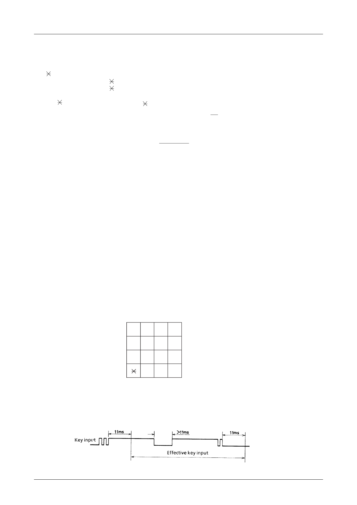
Key Debounce Time
• A key debounce circuit is built in key input to prevent misoperation caused by switch chattering.
Input is valid when on continuously for 11ms or more,
and is invalid when off continuously for 11ms or more.
No.3095–9/12
Share Link: 