LC75842E 查看數據表(PDF) - SANYO -> Panasonic
零件编号
产品描述 (功能)
生产厂家
LC75842E Datasheet PDF : 10 Pages
| |||
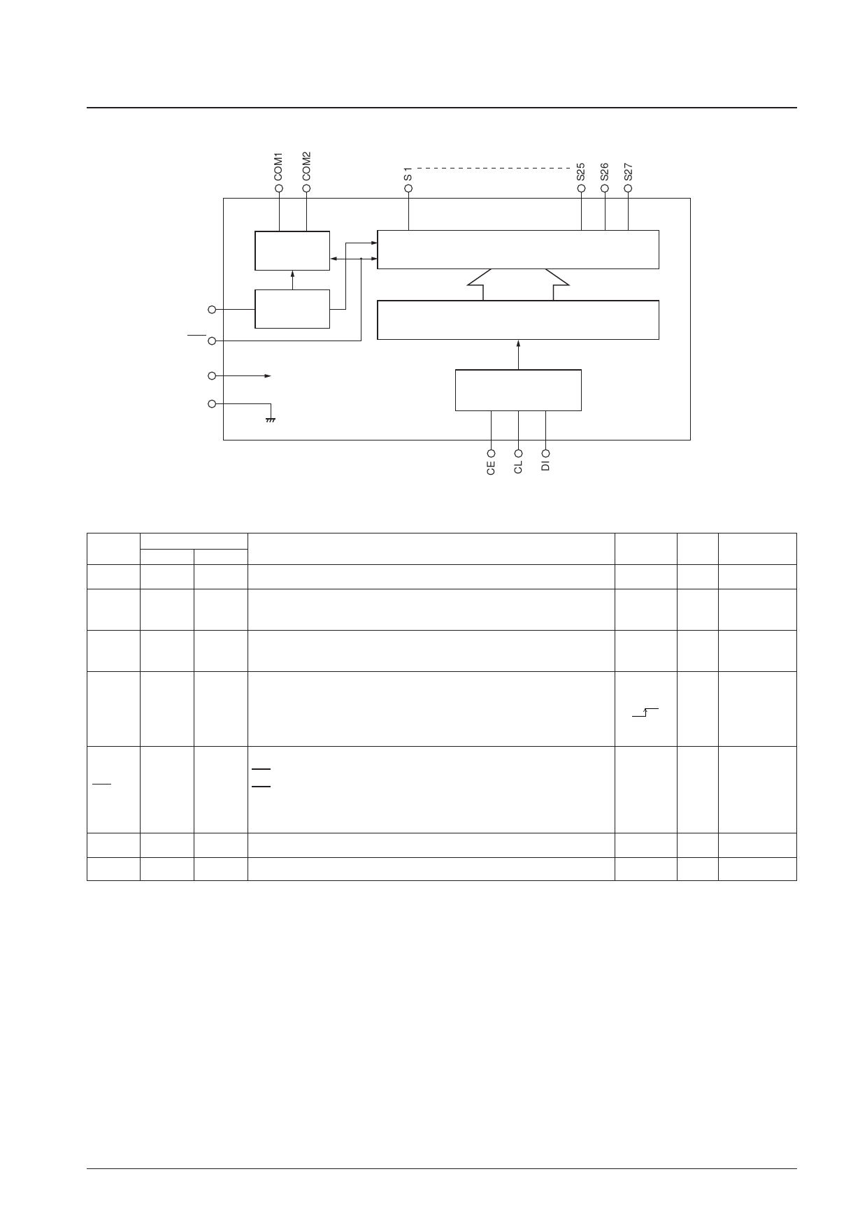
Block Diagram
LC75842E, LC75842M
OSC
INH
VDD
VSS
COMMON
DRIVER
CLOCK
GENERATOR
SEGMENT DRIVER & LATCH
SHIFT REGISTER
CCB INTERFACE
A03196
Pin Functions
Pin No.
Pin
LC75842E LC75842M
Function
S1 to S27 1 to 27 5 to 31 Segment outputs for displaying the display data transferred by serial data input.
COM1
36
COM2
35
4
Common driver outputs. The frame frequency fO is fOSC/512 Hz.
3
OSC
28
32
Oscillator connection. An oscillator circuit is formed by connecting an external
resistor and capacitor at this pin.
Active
—
—
—
CE
32
36
Serial data transfer inputs. Must be connected to the control microprocessor.
H
CL
33
1
CE: Chip enable
CL: Synchronization clock
DI
34
2
DI: Transfer data
—
Display off control input
INH = low (VSS) .....Display off (S1 to S27, COM1 and COM2 = low)
INH
30
34
INH = high (VDD)....Display on
L
However, serial data transfer is possible when the display is forced off by this
pin.
VDD
29
33 Power supply. Provide a power supply voltage of between 4.0 and 6.0 V.
—
VSS
31
35 Power supply. Connect this pin to ground.
—
Handling when
I/O
unused
O
Open
O
Open
I/O
VDD
I
GND
I
GND
—
—
—
—
No. 4966-4/10
Share Link: 