LE52C 查看數據表(PDF) - STMicroelectronics
零件编号
产品描述 (功能)
生产厂家
LE52C Datasheet PDF : 27 Pages
| |||
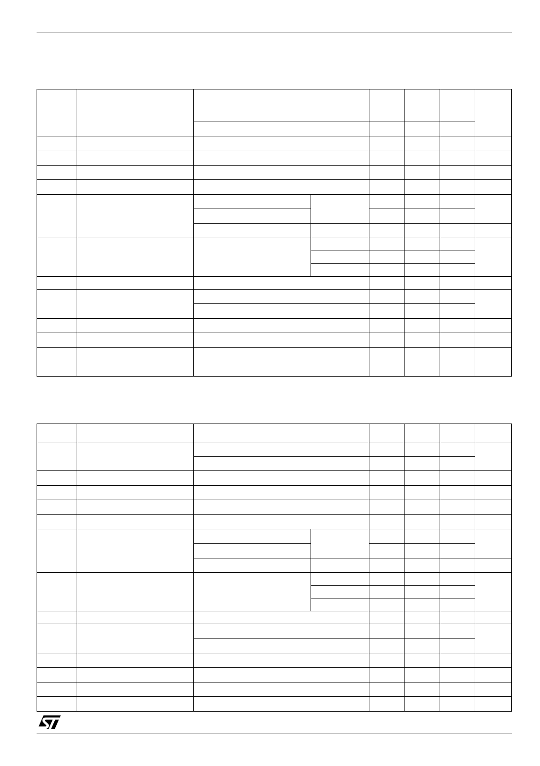
LE00AB/C SERIES
Table 10: Electrical Characteristics For LE27AB (refer to the test circuits, Tj = 25°C, CI = 0.1 µF,
CO = 2.2 µF unless otherwise specified.)
Symbol
Parameter
Test Conditions
Min. Typ. Max. Unit
VO Output Voltage
IO = 10 mA, VI = 4.7 V
2.673 2.7 2.727 V
IO = 10 mA, VI = 4.7 V, Ta = -25 to 85°C 2.646
2.754
VI Operating Input Voltage
IO = 100 mA
18
V
IO Output Current Limit
150
mA
∆VO Line Regulation
VI = 3.4 to 18 V,
IO = 0.5 mA
3
15
mV
∆VO Load Regulation
VI = 3.7 V
IO = 0.5 to 100 mA
3
15
mV
Id Quiescent Current
VI = 3.7 to 18V, IO = 0mA ON MODE
0.5
1
mA
VI = 3.7 to 18V, IO = 100mA
1.5
3
VI = 6 V
OFF MODE
50
100
µA
SVR Supply Voltage Rejection
IO = 5 mA
VI = 4.7 ± 1 V
f = 120 Hz
f = 1 KHz
82
dB
77
f = 10 KHz
60
eN Output Noise Voltage
B = 10 Hz to 100 KHz
50
µV
Vd Dropout Voltage
IO = 100 mA
0.2
0.4
V
IO = 100 mA
Ta = -40 to 125°C
0.5
VIL Control Input Logic Low
Ta = -40 to 125°C
0.8
V
VIH Control Input Logic High Ta = -40 to 125°C
2
V
II Control Input Current
VI = 6 V, VC = 6 V
10
µA
CO Output Bypass Capacitance ESR = 0.1 to 10 Ω
IO = 0 to 100 mA 2
10
µF
Table 11: Electrical Characteristics For LE27C (refer to the test circuits, Tj = 25°C, CI = 0.1 µF,
CO = 2.2 µF unless otherwise specified.)
Symbol
Parameter
Test Conditions
Min.
VO
VI
IO
∆VO
∆VO
Id
SVR
eN
Vd
VIL
VIH
II
CO
Output Voltage
Operating Input Voltage
Output Current Limit
IO = 10 mA, VI = 4.7 V
IO = 10 mA, VI = 4.7 V, Ta = -25 to 85°C
IO = 100 mA
Line Regulation
Load Regulation
Quiescent Current
Supply Voltage Rejection
VI = 3.4 to 18 V,
IO = 0.5 mA
VI = 3.7 V
IO = 0.5 to 100 mA
VI = 3.7 to 18V, IO = 0mA ON MODE
VI = 3.7 to 18V, IO = 100mA
VI = 6 V
OFF MODE
IO = 5 mA
VI = 4.7 ± 1 V
f = 120 Hz
f = 1 KHz
f = 10 KHz
Output Noise Voltage
B = 10 Hz to 100 KHz
Dropout Voltage
IO = 100 mA
IO = 100 mA
Control Input Logic Low
Ta = -40 to 125°C
Control Input Logic High Ta = -40 to 125°C
Control Input Current
VI = 6 V, VC = 6 V
Output Bypass Capacitance ESR = 0.1 to 10 Ω
Ta = -40 to 125°C
IO = 0 to 100 mA
2.646
2.592
150
2
2
Typ.
2.7
3
3
0.5
1.5
50
82
77
60
50
0.2
10
10
Max.
2.754
2.808
18
20
25
1
3
100
0.4
0.5
0.8
Unit
V
V
mA
mV
mV
mA
µA
dB
µV
V
V
V
µA
µF
7/27
Share Link: 