LM193AYD 查看數據表(PDF) - STMicroelectronics
零件编号
产品描述 (功能)
生产厂家
LM193AYD Datasheet PDF : 15 Pages
| |||
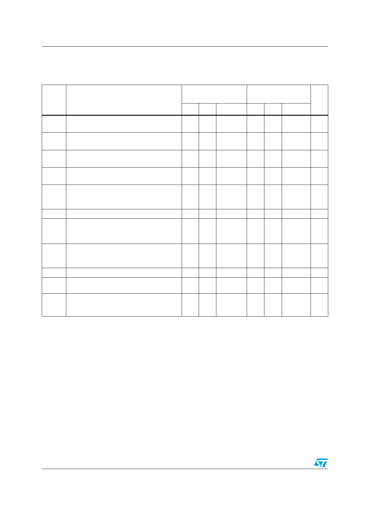
Electrical characteristics
LM193, LM293, LM393
3
Electrical characteristics
Table 3. VCC+ = +5V, VCC-= 0V, Tamb = +25°C (unless otherwise specified)
Symbol
Parameter
LM193A - LM293A
LM393A
LM193- LM293
LM393
Unit
Min. Typ. Max. Min Typ. Max.
Input offset voltage (1)
Vio
Tmin ≤ Tamb ≤ Tmax
Input offset current
Iio
Tmin ≤ Tamb ≤ Tmax
Input bias current (I+ or I-) (2)
Iib
Tmin ≤ Tamb ≤ Tmax
Large signal voltage gain
Avd VCC = 15V, RL = 15kΩ, Vo = 1V to 11V
Supply current (all comparators)
ICC
VCC = +5V, no load
VCC = +30V, no load
Vid Differential input voltage (3)
Low level output voltage
VOL Vid = -1V, Isink = 4mA
Tmin ≤ Tamb ≤ Tmax
High level output current
IOH VCC = Vo = 30V, Vid = 1V
Tmin ≤ Tamb ≤ Tmax
Isink Output sink current Vid= 1V, Vo = 1.5V
tre
Response time (4)
RL= 5.1kΩ connected to VCC+
Large signal response time
trel RL= 5.1kΩ connected to VCC+, el = TTL,
V(ref) = +1.4v
1
2
4
3
25
100
25
100
300
50 200
1
5
25
50 200
5
mV
9
50
nA
150
250
nA
400
V/mV
0.4
1
1
2.5
VCC+
250
400
700
0.1
1
6 16
1.3
0.4
1
mA
1
2.5
VCC+
250 400 mV
700
0.1
nA
1
μA
6 16
mA
1.3
μs
300
300
ns
1.
At output switch
VCC+ -1.5 V).
point,
Vo
≈
1.4 V, Rs = 0 with VCC+ from 5 V to 30 V, and over the full common-mode range (0 V to
2. The direction of the input current is out of the IC due to the PNP input stage. This current is essentially constant,
independent of the state of the output, so no loading charge exists on the reference of input lines.
3. The response time specified is for a 100 mV input step with 5 mV overdrive. For larger overdrive signals 300 ns can be
obtained.
4. Positive excursions of input voltage may exceed the power supply level. As long as the other voltage remains within the
common-mode range, the comparator will provide a proper output state. The low input voltage state must not be less than
-0.3 V (or 0.3 V below the negative power supply, if used).
4/15
Share Link: 