LT1032CN(RevC) 查看數據表(PDF) - Linear Technology
零件编号
产品描述 (功能)
生产厂家
LT1032CN Datasheet PDF : 8 Pages
| |||
LT1032
ABSOLUTE AXI U RATI GS
Supply Voltage ..................................................... ±15V
Logic Input Pins ............................................ V – to 25V
ON/OFF Pin ................................................. GND to 15V
Output (Forced) ............................. V – + 30V, V + – 30V
Response Pin.......................................................... ±6V
Short-Circuit Duration (to ±30V) .................... Indefinite
Operating Temperature Range
LT1032C ............................................... 0°C to 70°C
LT1032M ....................................... – 55°C to 125°C
Guaranteed Functional by Design .......... – 25°C to 85°C
Storage Temperature Range ................ – 65°C to 150°C
Lead Temperature (Soldering, 10 sec)................. 300°C
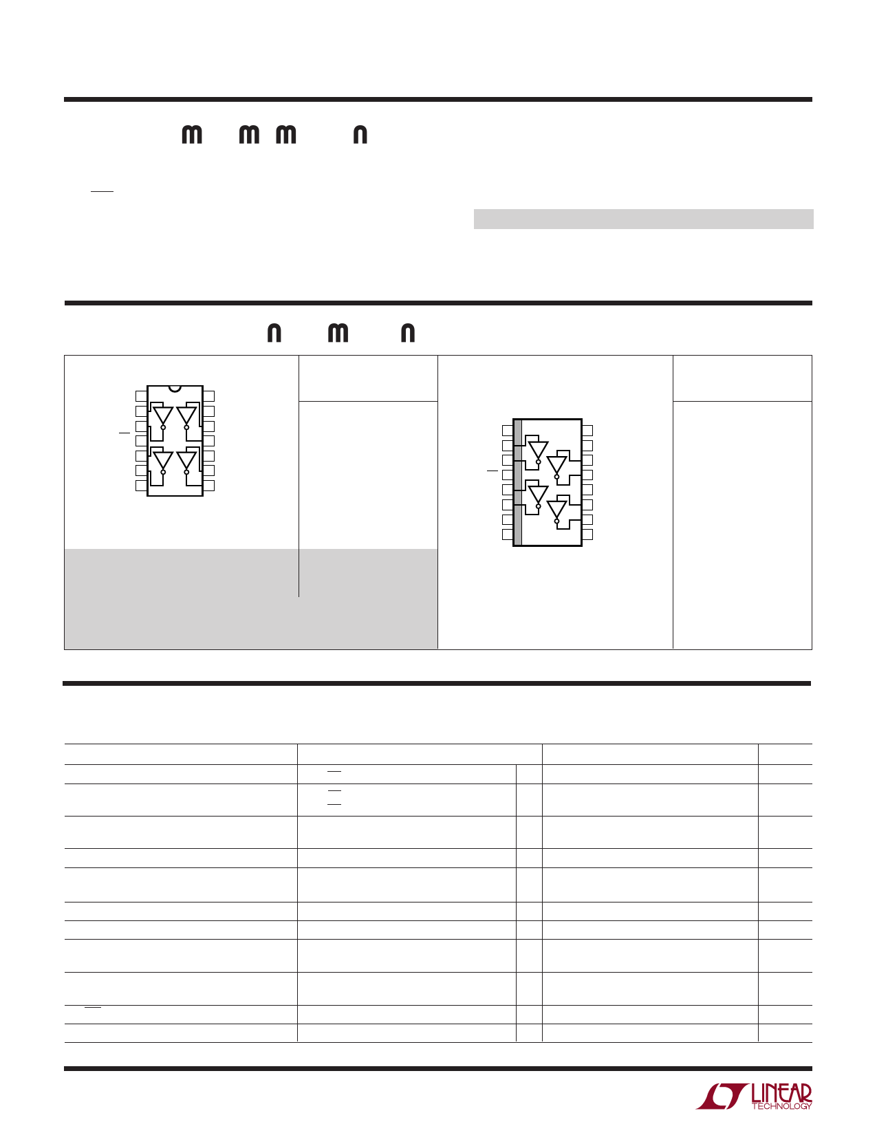
PACKAGE/ORDER I FOR ATIO
VEE 1
(–15V TO –5V)
2
3
ON/OFF
(0V TO 5V)
4
5
6
GND 7
TOP VIEW
14
VCC
(5V TO 15V)
13 STROBE
12
11
10
RESPONSE
CONTROL
9
8
J PACKAGE
N PACKAGE
14-LEAD CERAMIC DIP 14-LEAD PLASTIC DIP
TJMAX = 85°C, θJA = 100°C/W, θJC = 60°C (CJ)
TJMAX = 85°C, θJA = 100°C/W, θJC = 60°C (CN)
TJMAX = 150°C, θJA = 100°C/W, θJC = 60°C (MJ)
Consult factory for Industrial grade parts.
ORDER PART
NUMBER
LT1032CJ
LT1032CN
LT1032MJ
VEE 1
2
3
ON/OFF 4
5
6
GND 7
NC 8
TOP VIEW
16 VCC
15 STROBE
14
13
12
RESPONSE
CONTROL
11
10
9 NC
S PACKAGE
16-LEAD PLASTIC SOL
TJMAX = 85°C, θJA = 80°C/W
ORDER PART
NUMBER
LT1032CS
ELECTRICAL CHARACTERISTICS Supply Voltage = ±5V to ±15V
PARAMETER
Supply Current
Power Supply Leakage Current
Output Voltage Swing
Output Current (Active)
Output Current (Shutdown)
Output Overload Voltage (Forced)
Input Overload Voltage (Forced)
Logic Input Levels
Logic Input Current
ON/OFF Pin Current
Slew Rate
Change in Slew Rate (Note 2)
Response Pin Leakage
CONDITIONS
VON/OFF ≥ 2.4V, IOUT = 0, All Outputs Low q
VON/OFF ≤ 0.4V
VON/OFF ≤ 0.1V, TA = 125°C
q
Load = 2mA Positive
Negative
VSUPPLY = ±5V to ±15V
VSUPPLY = 0V, VOUT = ±30V
VSUPPLY = ±15V, VOUT = ±20V
Operating or Shutdown
q
Operating of Shutdown
q
Low Input (VOUT = High)
q
High Input (VOUT = Low)
q
VIN > 2.0V
VIN < 0.8V
0 ≤ VIN ≤ 5V
q
IRESPONSE = 0, RL = 3k
IRESPONSE = 50µA
IRESPONSE = – 50µA
VSUPPLY = ±6V, VON/OFF ≤ 0.4V
VRESPONSE = ±6V
MIN
V + – 0.3V
10
V + – 30V
V–
2
–10
4
TYP
500
1
10
V + – 0.1V
V – + 0.7V
22
2
2
1.4
1.4
2
10
3
15
50
– 50
1
MAX
1000
10
50
V – + 0.9V
100
100
V – + 30V
30V
0.8
20
20
50
30
UNITS
µA
µA
µA
V
V
mA
µA
µA
V
V
V
V
µA
µA
µA
V/µs
%
%
µA
The q denotes specifications which apply over the full operating
temperature range.
Note 1: 3V applied to the strobe pin will force all outputs low. Strobe pin
input impedance is about 2k to ground. Leave open when not used.
Note 2: Response can be changed by connecting a resistor to the supply.
For supplies less than ±6V this current is desconnected when shut down.
Leave open when not used.
2
Share Link: 