LT1191C 查看數據表(PDF) - Linear Technology
零件编号
产品描述 (功能)
生产厂家
LT1191C Datasheet PDF : 12 Pages
| |||
LT1191
ELECTRICAL CHARACTERISTICS The q denotes the specifications which apply over the full operating
temperature range of 0°C ≤ TA ≤ 70°C. VS = ±5V, Pin 5 open circuit unless otherwise noted.
SYMBOL PARAMETER
CONDITIONS
LT1191C
MIN TYP MAX
UNITS
VOS
Input Offset Voltage
N8 Package
SO-8 Package
q
2
6
mV
10
mV
∆VOS /∆T
IOS
IB
CMRR
PSRR
AVOL
Input VOS Drift
Input Offset Current
Input Bias Current
Common Mode Rejection Ratio
Power Supply Rejection Ratio
Large-Signal Voltage Gain
VOUT
IS
ISHDN
Output Voltage Swing
Supply Current
Shutdown Supply Current
Shutdown Pin Current
VCM = – 2.5V to 3.5V
VS = ± 2.375V to ± 5V
RL = 1k, VO = ± 3V
RL = 100, VO = ±3V
RL = 1k
Pin 5 at V – (Note 8)
Pin 5 at V –
q
8
q
0.2
1.7
q
±0.5 ±2.5
q 58
70
q 58
70
q 20
40
q3
9
q ±3.7 ±3.9
q
32
38
q
1.4
2.1
q
20
µV/°C
µA
µA
dB
dB
V/mV
V/mV
V
mA
mA
µA
Note 1: Absolute Maximum Ratings are those values beyond which the life
of the device may be impaired.
Note 2: A heat sink is required to keep the junction temperature below
absolute maximum when the output is shorted.
Note 3: Exceeding the input common mode range may cause the output to
invert.
Note 4: Slew rate is measured between ±1V on the output, with a ±1.5V
input step.
Note 5: Full-power bandwidth is calculated from the slew rate
measurement:
FPBW = SR/2πVP.
Note 6: Settling time measurement techniques are shown in “Take the
Guesswork Out of Settling Time Measurements,” EDN, September 19,
1985. AV = –1, RL = 1k.
Note 7: NTSC (3.58MHz). For RL = 1k, Diff AV = 0.07%, Diff Ph = 0.02°.
Note 8: See Applications section for shutdown at elevated temperatures.
Do not operate the shutdown above TJ > 125°C.
Note 9: AC parameters are 100% tested on the ceramic and plastic DIP
packaged parts (J and N suffix) and are sample tested on every lot of the
SO packaged parts (S suffix).
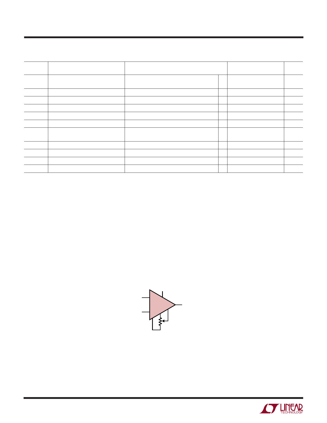
Optional Offset Nulling Circuit
5V
3+
7
LT1191
2–
8
1
6
4
–5V
INPUT OFFSET VOLTAGE CAN BE ADJUSTED OVER A ±100mV
RANGE WITH A 1kΩ TO 10kΩ POTENTIOMETER
LT1191 • TA03
4
Share Link: 