LT1310 查看數據表(PDF) - Linear Technology
零件编号
产品描述 (功能)
生产厂家
LT1310 Datasheet PDF : 12 Pages
| |||
LT1310
PI FU CTIO S
FB (Pin 1): Feedback Pin for Error Amplifier. Connect the
resistor divider here to set output voltage according to
the formula:
VOUT = 1.255(1 + R1/R2)
VOUT
R1
FB
R2
Minimize trace area at this pin.
SHDN (Pin 2): Shutdown Pin. For active mode, tie this pin
to a voltage between 2.4V and 18V. To disable the part and
go into low current mode, pull this pin below 0.4V.
PLL-LPF (Pin 3): Phase Locked-Loop Filter Pin. This is the
output of the phase detector and also the input to the
voltage controlled oscillator (VCO). Connect an RC filter
here. Typically, R = 3k and C = 1500pF. The voltage range
at the PLL-LPF pin is approximately 0V to 1.5V with 1.5V
corresponding to the maximum switching frequency. For
applications not requiring synchronization, use a pull-up
resistor at this pin; the pull-up voltage must be above 2.4V.
Set the pull-up resistor value according to:
( ) RPULLUP =
VPULLUP – 1.5V
300µA
For a pull-up voltage of 5V:
RPULLUP
=
(5V – 1.5V)
300µA
≈
11.6k
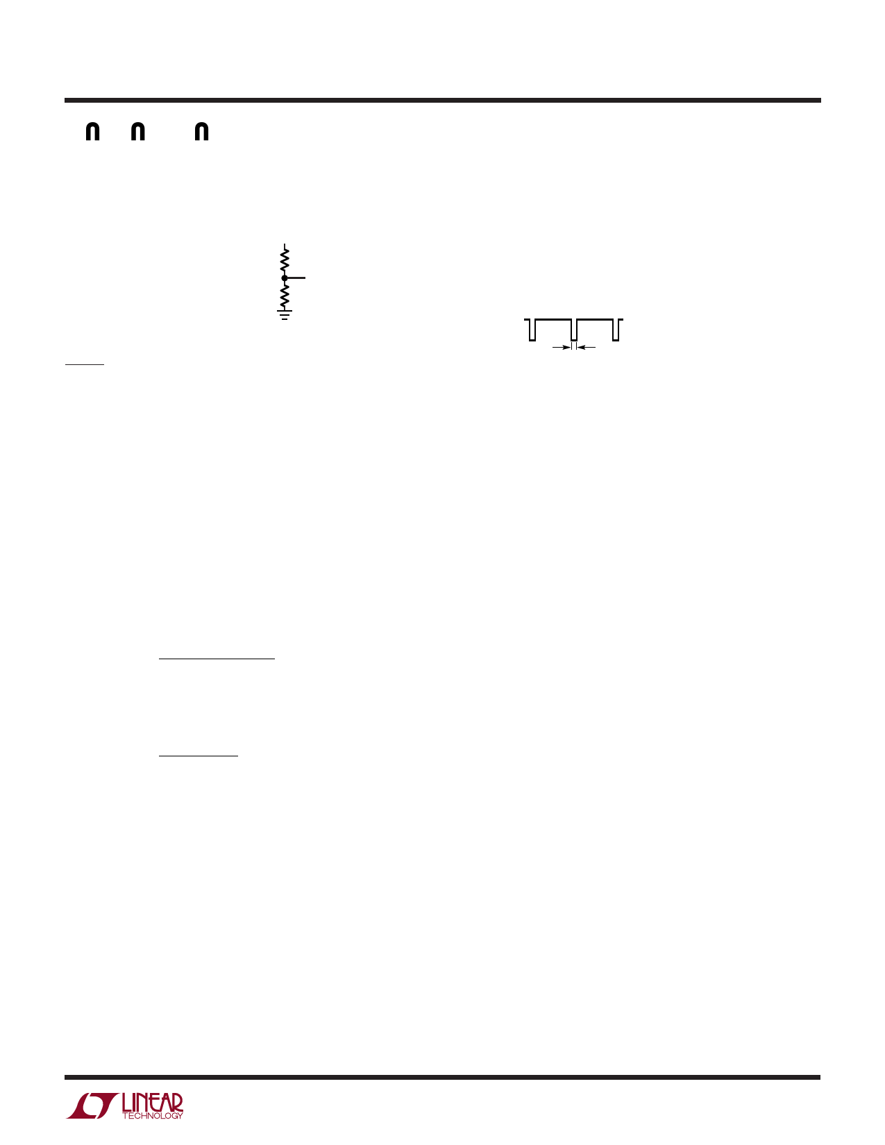
SYNC (Pin 4): Frequency Synchronization Pin. Inject the
external synchronizing signal here. The phase detector is
edge triggered and when locked the rising edge of the
sync signal will be aligned with the turn-on of the power
transistor. The SYNC signal must have a minimum HIGH
amplitude of 1.2V and a maximum LOW amplitude of
0.2V with the signal staying low for at least 100ns.
1.2V (MIN)
0.2V (MAX)
100ns (MIN)
GND (Pin 5, Exposed Pad): Ground. Tie both Pin 5 and
the exposed pad directly to local ground plane. The
ground metal to the exposed pad should be wide for better
heat dissipation. Multiple vias (local ground plane ↔
ground backplane) placed close to the exposed pad can
further aid in reducing thermal resistance. The exposed
pad must be soldered to ground for the LT1310 to function
properly.
SW (Pins 6, 7): Switch Pin. Must tie Pin 6 to Pin 7.
Connect inductor/diode here. Minimize trace area at this
pin to keep EMI down.
VIN (Pin 8): Supply Pin. Must be bypassed as close as
possible to the pin.
CT (Pin 9): Timing Capacitor Pin for VCO. Place the timing
capacitor from this pin to ground to set the frequency
range for the oscillator. Minimize trace at this pin to reduce
stray capacitance.
VC (Pin 10): Compensation Pin for Error Amplifier. Tie an
RC network here to compensate the voltage feedback
loop.
sn1310 1310fs
5
Share Link: 