LT1370 查看數據表(PDF) - Linear Technology
零件编号
产品描述 (功能)
生产厂家
LT1370 Datasheet PDF : 16 Pages
| |||
U
OPERATION
Unique error amplifier circuitry allows the LT1370 to
directly regulate negative output voltages. The negative
feedback amplifier’s 100k source resistor is brought out
for negative output voltage sensing. The NFB pin regulates
at – 2.48V while the amplifier output internally drives the
FB pin to 1.245V. This architecture, which uses the same
main error amplifier, prevents duplicating functions and
maintains ease of use. Consult LTC Marketing for units
that can regulate down to – 1.25V.
The error signal developed at the amplifier output is
brought out externally. This pin (VC) has three different
LT1370
functions. It is used for frequency compensation, current
limit adjustment and soft starting. During normal regula-
tor operation this pin sits at a voltage between 1V (low
output current) and 1.9V (high output current). The error
amplifier is a current output (gm) type, so this voltage can
be externally clamped for lowering current limit. Like-
wise, a capacitor coupled external clamp will provide soft
start. Switch duty cycle goes to zero if the VC pin is pulled
below the control pin threshold, placing the LT1370 in an
idle mode.
UU W U
APPLICATIO S I FOR ATIO
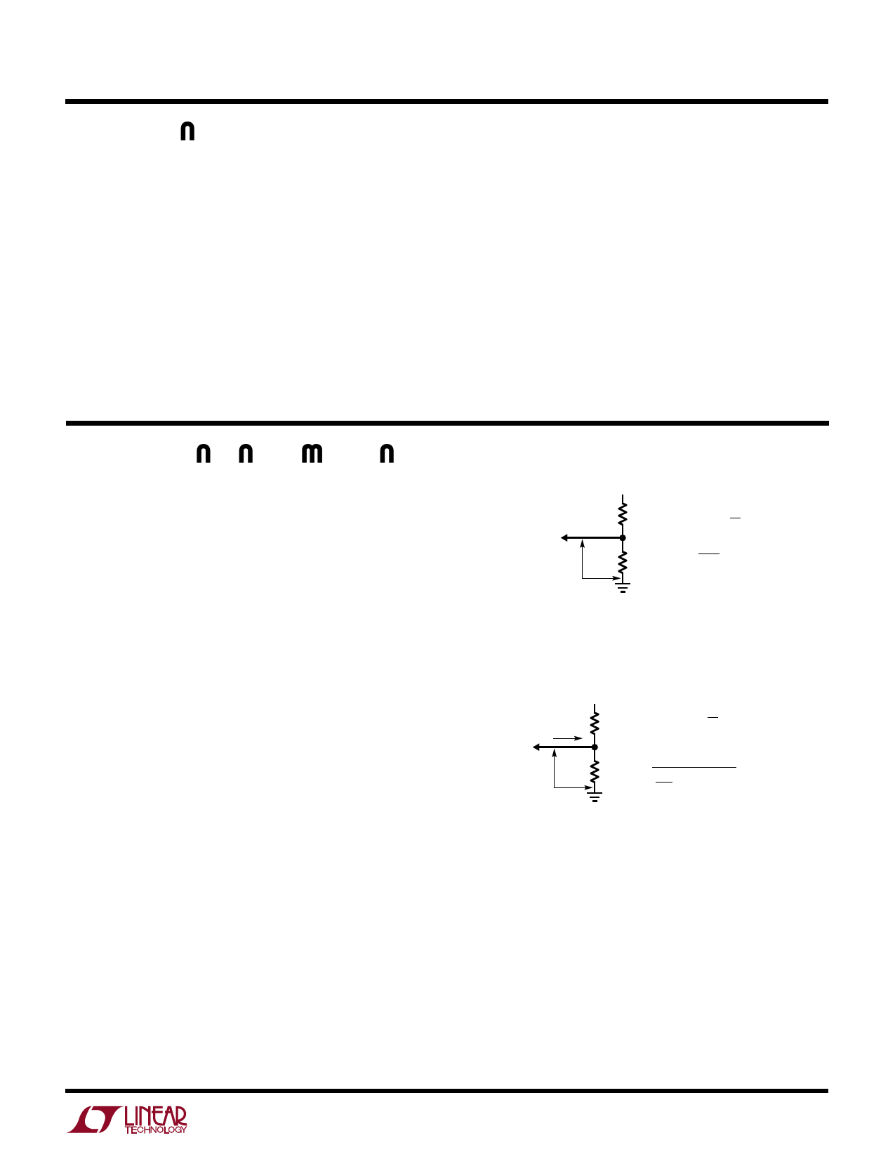
Positive Output Voltage Setting
The LT1370 develops a 1.245V reference (VREF) from the
FB pin to ground. Output voltage is set by connecting the
FB pin to an output resistor divider (Figure 1). The FB pin
bias current represents a small error and can usually be
ignored for values of R2 up to 7k. The suggested value for
R2 is 6.19k. The NFB pin is normally left open for positive
output applications. Positive fixed voltage versions are
available (consult LTC Marketing).
Negative Output Voltage Setting
The LT1370 develops a – 2.48V reference (VNFR) from the
NFB pin to ground. Output voltage is set by connecting the
NFB pin to an output resistor divider (Figure 2). The
–30µA NFB pin bias current (INFB) can cause output
voltage errors and should not be ignored. This has been
accounted for in the formula in Figure 2. The suggested
value for R2 is 2.49k. The FB pin is normally left open for
negative output applications.
Dual Polarity Output Voltage Sensing
Certain applications benefit from sensing both positive
and negative output voltages. One example is the “Dual
Output Flyback Converter with Overvoltage Protection”
circuit shown in the Typical Applications section. Each
output voltage resistor divider is individually set as
described above. When both the FB and NFB pins are used,
FB
PIN
VREF
VOUT
R1
R2
( ) VOUT = VREF
1
+
R1
R2
( ) R1 = R2
VOUT
1.245
–1
LT1370 • F01
Figure 1. Positive Output Resistor Divider
–VOUT
INFB
R1
NFB
PIN
R2
VNFR
( ) –VOUT = VNFB
1
+
R1
R2
+ INFB (R1)
( ) ( ) R1 = VOUT– 2.48
2.48 + 30 • 10–6
R2
LT1370 • F02
Figure 2. Negative Output Resistor Divider
the LT1370 acts to prevent either output from going
beyond its set output voltage. For example, in this applica-
tion if the positive output were more heavily loaded than
the negative, the negative output would be greater and
would regulate at the desired set-point voltage. The posi-
tive output would sag slightly below its set-point voltage.
This technique prevents either output from going unregu-
lated high at no load.
7
Share Link: 