LT1377CS8 查看數據表(PDF) - Linear Technology
零件编号
产品描述 (功能)
生产厂家
LT1377CS8 Datasheet PDF : 12 Pages
| |||
LT1372/LT1377
UU W U
APPLICATIO S I FOR ATIO
Frequency Compensation
Loop frequency compensation is performed on the output
of the error amplifier (VC pin) with a series RC network.
The main pole is formed by the series capacitor and the
output impedance (≈500kΩ) of the error amplifier. The
pole falls in the range of 2Hz to 20Hz. The series resistor
creates a “zero” at 1kHz to 5kHz, which improves loop
stability and transient response. A second capacitor,
typically one-tenth the size of the main compensation
capacitor, is sometimes used to reduce the switching
frequency ripple on the VC pin. VC pin ripple is caused by
output voltage ripple attenuated by the output divider and
multiplied by the error amplifier. Without the second
capacitor, VC pin ripple is:
(magnetic) radiation is minimized by keeping output di-
ode, switch pin, and output bypass capacitor leads as
short as possible. E field radiation is kept low by minimiz-
ing the length and area of all traces connected to the switch
pin. A ground plane should always be used under the
switcher circuitry to prevent interplane coupling.
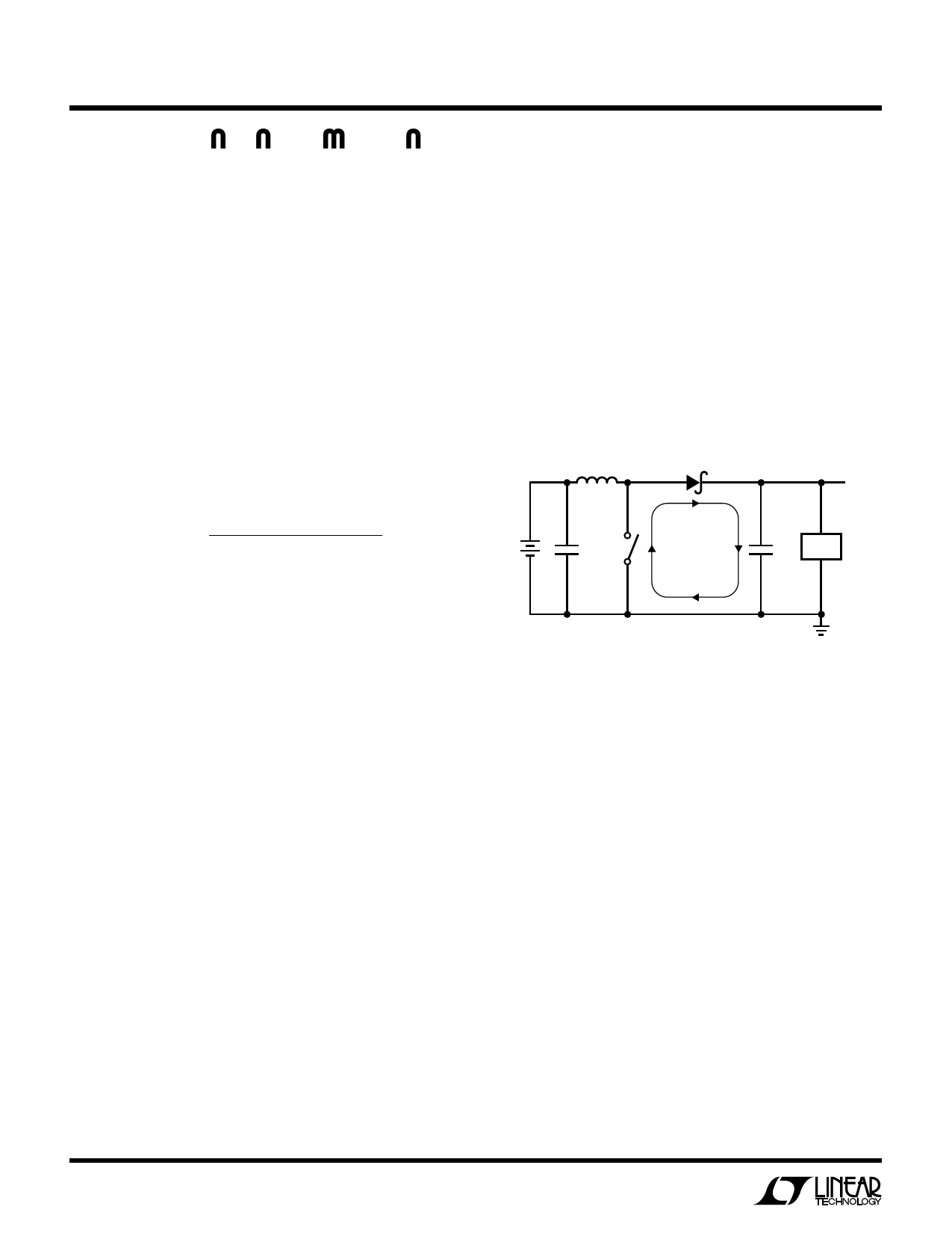
The high speed switching current path is shown schemati-
cally in Figure 3. Minimum lead length in this path is
essential to ensure clean switching and low EMI. The path
including the switch, output diode, and output capacitor is
the only one containing nanosecond rise and fall times.
Keep this path as short as possible.
SWITCH
L1 NODE
VOUT
VC
Pin
Ripple
=
1.245(VRIPPLE)(gm)(RC)
(VOUT)
VRIPPLE = Output ripple (VP–P)
gm = Error amplifier transconductance
( ≈1500µmho)
RC = Series resistor on VC pin
VOUT = DC output voltage
To prevent irregular switching, VC pin ripple should be
kept below 50mVP–P. Worst-case VC pin ripple occurs at
maximum output load current and will also be increased
if poor quality (high ESR) output capacitors are used. The
addition of a 0.0047µF capacitor on the VC pin reduces
switching frequency ripple to only a few millivolts. A low
value for RC will also reduce VC pin ripple, but loop phase
margin may be inadequate.
HIGH
VIN
FREQUENCY
LOAD
CIRCULATING
PATH
Figure 3
LT1372 • F03
More Help
For more detailed information on switching regulator
circuits, please see Application Note 19. Linear Technol-
ogy also offers a computer software program, SwitcherCAD,
to assist in designing switching converters. SwitcherCAD
will be updated in late 1995 for the LT1372 and LT1377. In
addition, our applications department is always ready to
lend a helping hand.
Switch Node Considerations
For maximum efficiency, switch rise and fall time are
made as short as possible. To prevent radiation and high
frequency resonance problems, proper layout of the com-
ponents connected to the switch node is essential. B field
10
Share Link: 