LT1800IS8-TRPBF жҹҘзңӢж•ёж“ҡиЎЁпјҲPDFпјү - Linear Technology
йӣ¶д»¶зј–еҸ·
дә§е“ҒжҸҸиҝ° (еҠҹиғҪ)
з”ҹдә§еҺӮ家
LT1800IS8-TRPBF
Linear Technology

LT1800IS8-TRPBF Datasheet PDF : 18 Pages
| |||
ELECTRICAL CHARACTERISTICS
Note 1: Stresses beyond those listed under Absolute Maximum Ratings
may cause permanent damage to the device. Exposure to any Absolute
Maximum Rating condition for extended periods may affect device
reliability and lifetime.
Note 2: The inputs are protected by back-to-back diodes and by ESD
diodes to the supply rails. If the differential input voltage exceeds 1.4V or
either input goes outside the rails, the input current should be limited to
less than 10mA.
Note 3: A heat sink may be required to keep the junction temperature
below the absolute maximum rating when the output is shorted
indeп¬Ғnitely.
LT1800
Note 4: The LT1800C/LT1800I are guaranteed functional over the
temperature range of вҖ“40В°C to 85В°C.
Note 5: The LT1800C is guaranteed to meet speciп¬Ғed performance from
0В°C to 70В°C. The LT1800C is designed, characterized and expected to
meet speciп¬Ғed performance from вҖ“40В°C to 85В°C but is not tested or
QA sampled at these temperatures. The LT1800I is guaranteed to meet
speciп¬Ғed performance from вҖ“40В°C to 85В°C.
Note 6: Minimum supply voltage is guaranteed by power supply rejection
ratio test.
Note 7: Output voltage swings are measured between the output and
power supply rails.
Note 8: This parameter is not 100% tested.
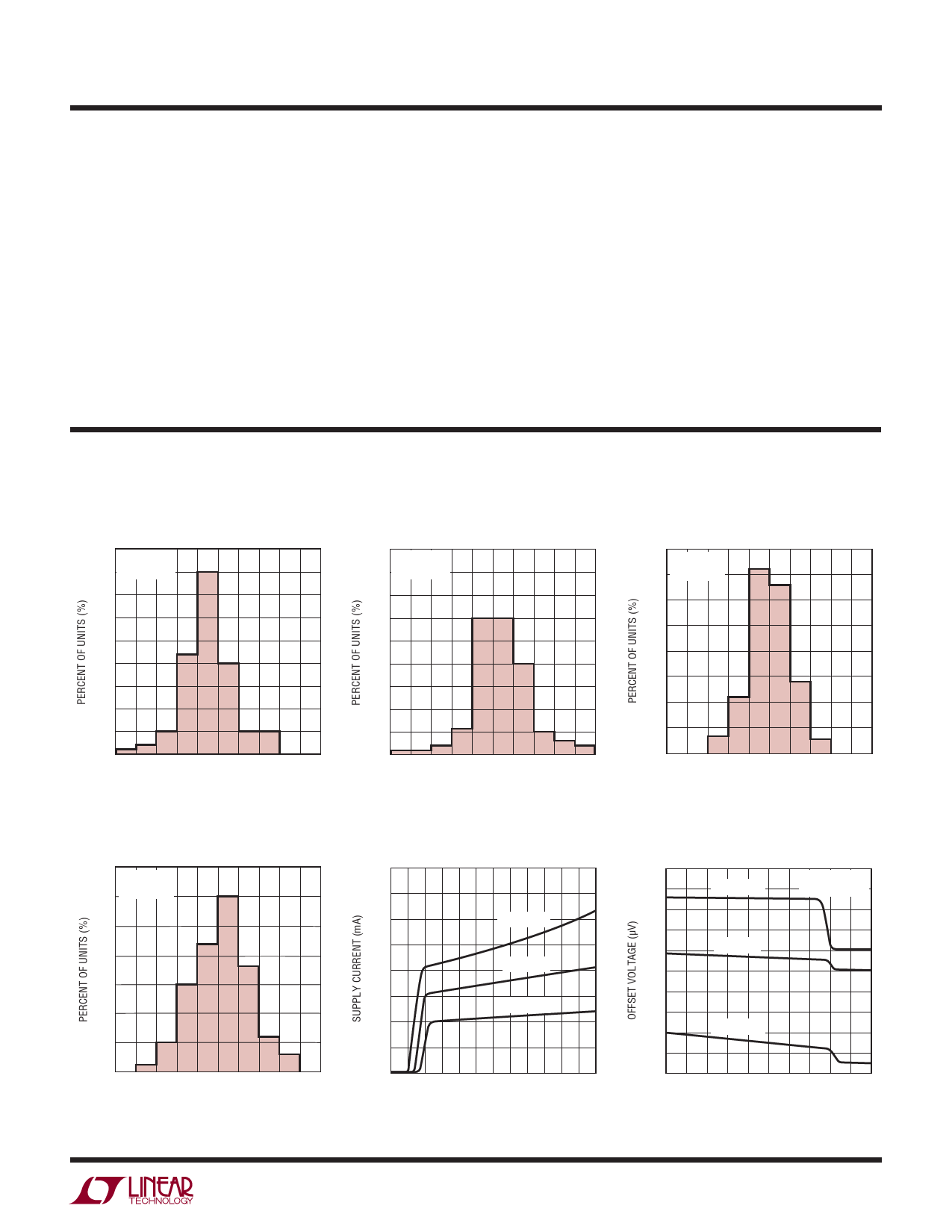
TYPICAL PERFORMANCE CHARACTERISTICS
VOS Distribution, VCM = 0V
(SO-8, PNP Stage)
45
VS = 5V, 0V
40 VCM = 0V
35
30
25
20
15
10
5
0
вҖ“250 вҖ“150 вҖ“50 50 150 250
INPUT OFFSET VOLTAGE (ОјV)
1800 G01
VOS Distribution, VCM = 5V
(SOT-23, NPN Stage)
35
VS = 5V, 0V
30 VCM = 5V
25
20
15
10
5
0
вҖ“2500 вҖ“1500 вҖ“500 500 1500
INPUT OFFSET VOLTAGE (ОјV)
2500
1800 G04
VOS Distribution, VCM = 5V
(SO-8, NPN Stage)
45
VS = 5V, 0V
40 VCM = 5V
35
30
25
20
15
10
5
0
вҖ“2000
вҖ“1200 вҖ“400 400 1200 2000
INPUT OFFSET VOLTAGE (ОјV)
1800 G02
Supply Current vs Supply Voltage
4
3
TA = 125В°C
2
TA = 25В°C
TA = вҖ“55В°C
1
0
0 1 2 3 4 5 6 7 8 9 10 11 12
TOTAL SUPPLY VOLTAGE (V)
1800 G05
VOS Distribution, VCM = 0V
(SOT-23, PNP Stage)
40
VS = 5V, 0V
35 VCM = 0V
30
25
20
15
10
5
0
вҖ“1250
вҖ“750 вҖ“250 250 750
INPUT OFFSET VOLTAGE (ОјV)
1250
1800 G03
Offset Voltage
vs Input Common Mode Voltage
500
VS = 5V, 0V
400
TA = вҖ“55В°C
TYPICAL PART
300
200
100
TA = 25В°C
0
вҖ“100
вҖ“200
вҖ“300
TA = 125В°C
вҖ“400
вҖ“500
0
1
2
3
4
5
INPUT COMMON MODE VOLTAGE (V)
1800 G06
1800fa
7
Share Link: