LT3050MPMSE 查看數據表(PDF) - Linear Technology
零件编号
产品描述 (功能)
生产厂家
LT3050MPMSE
Linear Technology

LT3050MPMSE Datasheet PDF : 26 Pages
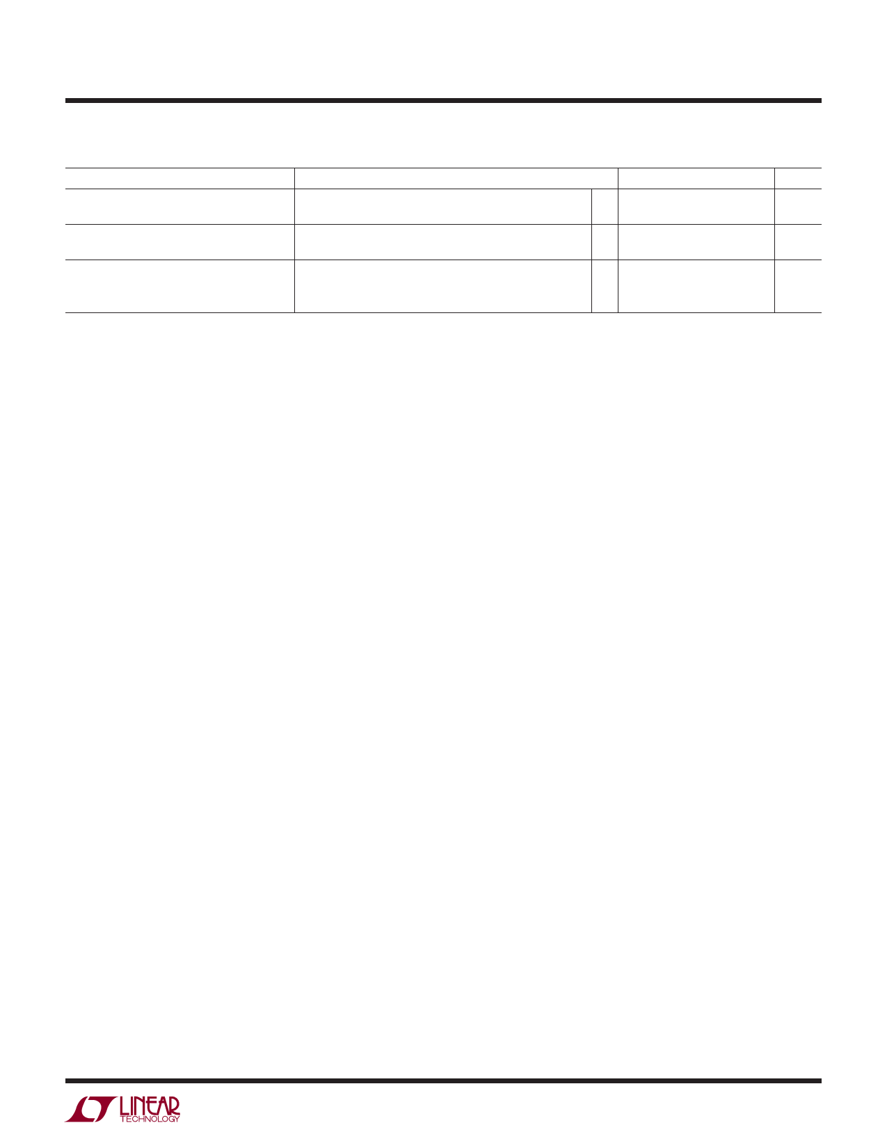
| |||
LT3050 Series
ELECTRICAL CHARACTERISTICS The l denotes the specifications which apply over the full operating
temperature range, otherwise specifications are at TA = 25°C. (Note 2)
PARAMETER
Minimum IMIN Threshold Accuracy
(Notes 6, 9)
IMIN Threshold Accuracy (Notes 6, 9)
Current Monitor Ratio (Notes 6, 10)
Ratio = IOUT/IMON
CONDITIONS
LT3050-3.3: 3.9V < VIN < 13.3V, RIMIN = 110K
LT3050, LT3050-5: 5.6V < VIN < 15V, RIMIN = 110K
LT3050-3.3: 3.9V < VIN < 13.3V, RIMIN = 11.3K
LT3050, LT3050-5: 5.6V < VIN < 15V, RIMIN = 11.3K
ILOAD = 5mA, 25mA, 50mA, 75mA, 100mA
LT3050-3.3: VIMON = VOUT, 3.9V < VIN < 13.3V
LT3050, LT3050-5: VIMON = VOUT, 5.6V < VIN < 15V
MIN TYP MAX UNITS
l 0.92 1.03 1.13
mA
l 0.9
1
1.1
mA
l 9.2
10.3 11.3
mA
l
9
10
11
mA
l 95
l 95
100
105
100
105
Note 1: Stresses beyond those listed under Absolute Maximum Ratings
may cause permanent damage to the device. Exposure to any Absolute
Maximum Rating condition for extended periods may affect device
reliability and lifetime. Absolute maximum input-to-output differential
voltage is not achievable with all combinations of rated IN pin and OUT pin
voltages. With the IN pin at 50V, the OUT pin may not be pulled below 0V.
The total differential voltage from IN to OUT must not exceed ±50V.
Note 2: The LT3050 is tested and specified under pulse load conditions
such that TJ ~ TA. The LT3050E is 100% production tested at TA = 25°C.
Performance at –40°C and 125°C is assured by design, characterization
and correlation with statistical process controls. The LT3050I is
guaranteed over the full –40°C to 125°C operating junction temperature
range. The LT3050MP is 100% tested over the –55°C to 125°C operating
junction temperature range.
Note 3: The LT3050 adjustable version is tested and specified for these
conditions with ADJ pin connected to the OUT pin.
Note 4: Maximum junction temperature limits operating conditions.
Regulated output voltage specifications do not apply for all possible
combinations of input voltage and output current. If operating at the
maximum input voltage, limit the output current range. If operating at the
maximum output current, limit the input voltage range.
Note 5: Dropout voltage is the minimum differential IN-to-OUT voltage
needed to maintain regulation at a specified output current. In dropout,
the output voltage equals (VIN - VDROPOUT). For some output voltages,
minimum input voltage requirements limit dropout voltage.
Note 6: To satisfy minimum input voltage requirements, the LT3050
adjustable version is tested and specified for these conditions with an
external resistor divider (60k bottom, 440k top) which sets VOUT to 5V.
The external resistor divider adds 10μA of DC load on the output. This
external current is not factored into GND pin current.
Note 7: GND pin current is tested with VIN = VOUT(NOMINAL) + 0.6V and
a current source load. GND pin current increases in dropout. For the
fixed output voltage versions, an internal resistor divider adds about
10μA to GND pin current. See the GND Pin Current curves in the Typical
Performance Characteristics section.
Note 8: Current limit varies inversely with the external resistor value tied
from the IMAX pin to GND. For detailed information on how to set the
IMAX pin resistor value, please see the Operation section. If a programmed
current limit is not needed, the IMAX pin must be tied to GND and internal
protection circuitry implements short-circuit protection as specified.
Note 9: The IMIN fault condition asserts if the output current falls below the
IMIN threshold defined by an external resistor from the IMIN pin to GND.
For detailed information on how to set the IMIN pin resistor value, please
see the Operation section. IMIN settings below the Minimum IMIN Accuracy
specification in the Electrical Characteristics section are not guaranteed
to ± 10% tolerance. If the IMIN fault condition is not needed, the IMIN pin
must be left floating (unconnected).
Note 10: The current monitor ratio varies slightly when VIMON ≠ VOUT. For
detailed information on how to calculate the output current from the IMON
pin, please see the Operation section. If the current monitor function is not
needed, the IMON pin must be tied to GND.
Note 11: To satisfy requirements for minimum input voltage, current limit
is tested at VIN = VOUT(NOMINAL) +1V or VIN = 2.2V, whichever is greater.
Note 12: ADJ pin bias current flows out of the ADJ pin:
Note 13: SHDN pin current flows into the SHDN pin.
Note 14: Reverse output current is tested with the IN pin grounded and the
OUT pin forced to the specified voltage. This current flows into the OUT pin
and out of the GND pin.
Note 15: 100mA of output current does not apply to the full range of input
voltage due to the internal current limit foldback.
Note 16: The ADJ pin cannot be externally driven for fixed output voltage
options. LTC allows the use of a small feedforward capacitor from OUT
to ADJ to reduce noise and improve transient response. See the Bypass
Capacitance section of the Applications Information.
3050fa
5
Share Link: