LT3682EDD 查看數據表(PDF) - Linear Technology
零件编号
产品描述 (功能)
生产厂家
LT3682EDD Datasheet PDF : 24 Pages
| |||
LT3682
ABSOLUTE MAXIMUM RATINGS
(Note 1)
VIN, RUN/SS Voltage (Note 2) …….…………….....60V
BOOST Pin Voltage …………………………..…….50V
BOOST Pin Above SW Pin …………………..……..30V
FB, RT, VC Voltage ......................................................5V
SYNC …………………………….………….……. 20V
BD and PG Voltage ..…….………………..……….. 30V
Operating Junction Temperature Range (Notes 3 and 6)
LT3682E ……………….…………... −40°C to 125°C
LT3682I ……………………………. −40°C to 125°C
Storage Temperature Range …………..−65°C to 150°C
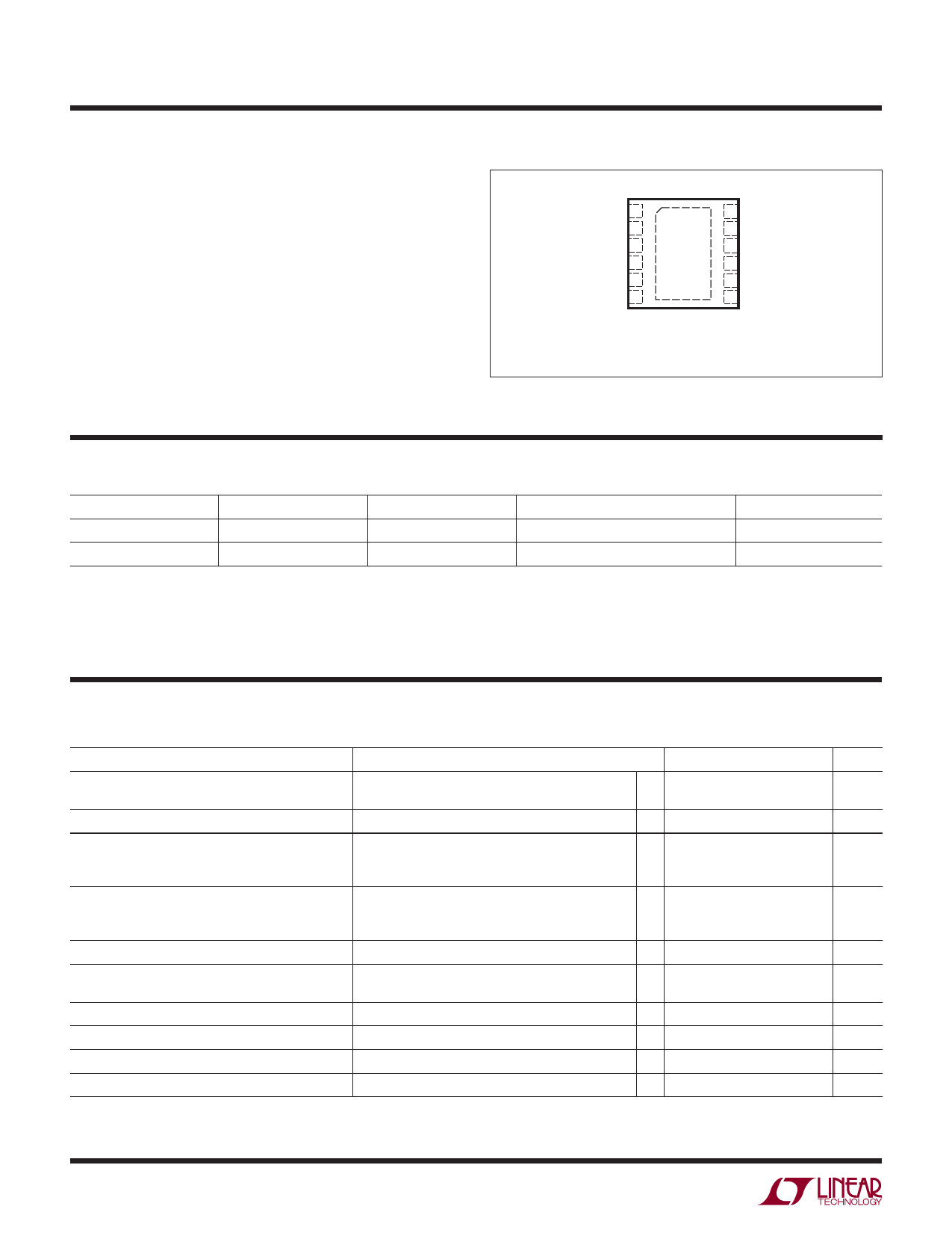
PIN CONFIGURATION
TOP VIEW
VC 1
FB 2
PG 3
GND 4
BD 5
BOOST 6
12 VIN
11 SYNC
13
10 RT
9 RUN/SS
8 SW
7 DA
DD PACKAGE
12-LEAD (3mm s 3mm) PLASTIC DFN
θJA = 43°C/W
EXPOSED PAD (PIN 13) IS PGND, MUST BE SOLDERED TO PCB
ORDER INFORMATION
LEAD FREE FINISH
TAPE AND REEL
PART MARKING*
PACKAGE DESCRIPTION
TEMPERATURE RANGE
LT3682EDD#PBF
LT3682EDD#TRPBF
LFDW
12-Lead (3mm × 3mm) Plastic DFN –40°C to 125°C
LT3682IDD#PBF
LT3682IDD#TRPBF
LFDW
12-Lead (3mm × 3mm) Plastic DFN –40°C to 125°C
Consult LTC Marketing for parts specified with wider operating temperature ranges. *The temperature grade is identified by a label on the shipping container.
Consult LTC Marketing for information on non-standard lead based finish parts.
For more information on lead free part marking, go to: http://www.linear.com/leadfree/
For more information on tape and reel specifications, go to: http://www.linear.com/tapeandreel/
ELECTRICAL CHARACTERISTICS The l denotes specifications which apply over the full operating temperature
range, otherwise specifications are at TA = 25°C, VIN = 10V, VRUN/SS = 10V, VBD = 3.3V unless otherwise noted. (Note 3)
PARAMETER
CONDITIONS
MIN TYP MAX UNITS
Minimum Operating Voltage
VIN Overvoltage Lockout
Quiescent Current from VIN
Quiescent Current from BD Pin
Minimum BD Pin Voltage
VBD = 3.3V
VBD < 3.0V
VRUN/SS = 0.2V
VRUN/SS = 10V, VBD = 3.3V, Not Switching
VRUN/SS = 10V, VBD = 0V, Not Switching
VRUN/SS = 0.2V
VRUN/SS = 10V, VBD = 3.3V, Not Switching
VRUN/SS = 10V, VBD = 0V, Not Switching
l
3.4
3.6
V
l
3.4
4.3
V
l 36
39
41
V
0.01 0.5
μA
l
35
60
μA
90
160
μA
0.01 0.5
μA
l
55
100
μA
0
5
μA
2.8
3
V
Feedback Voltage
792
800
808
mV
l 780
800
812
mV
FB Pin Bias Current (Note 4)
FB Pin Voltage = 800mV
l
5
80
nA
FB Voltage Line Regulation
3.6V < VIN < 36V
0.001 0.005
%/V
Error Amp gm
Error Amp Voltage Gain
IVC = ±1.5μA
430
μS
1300
V/V
3682f
2
Share Link: 