LT3685E 查看數據表(PDF) - Linear Technology
零件编号
产品描述 (功能)
生产厂家
LT3685E Datasheet PDF : 24 Pages
| |||
LT3685
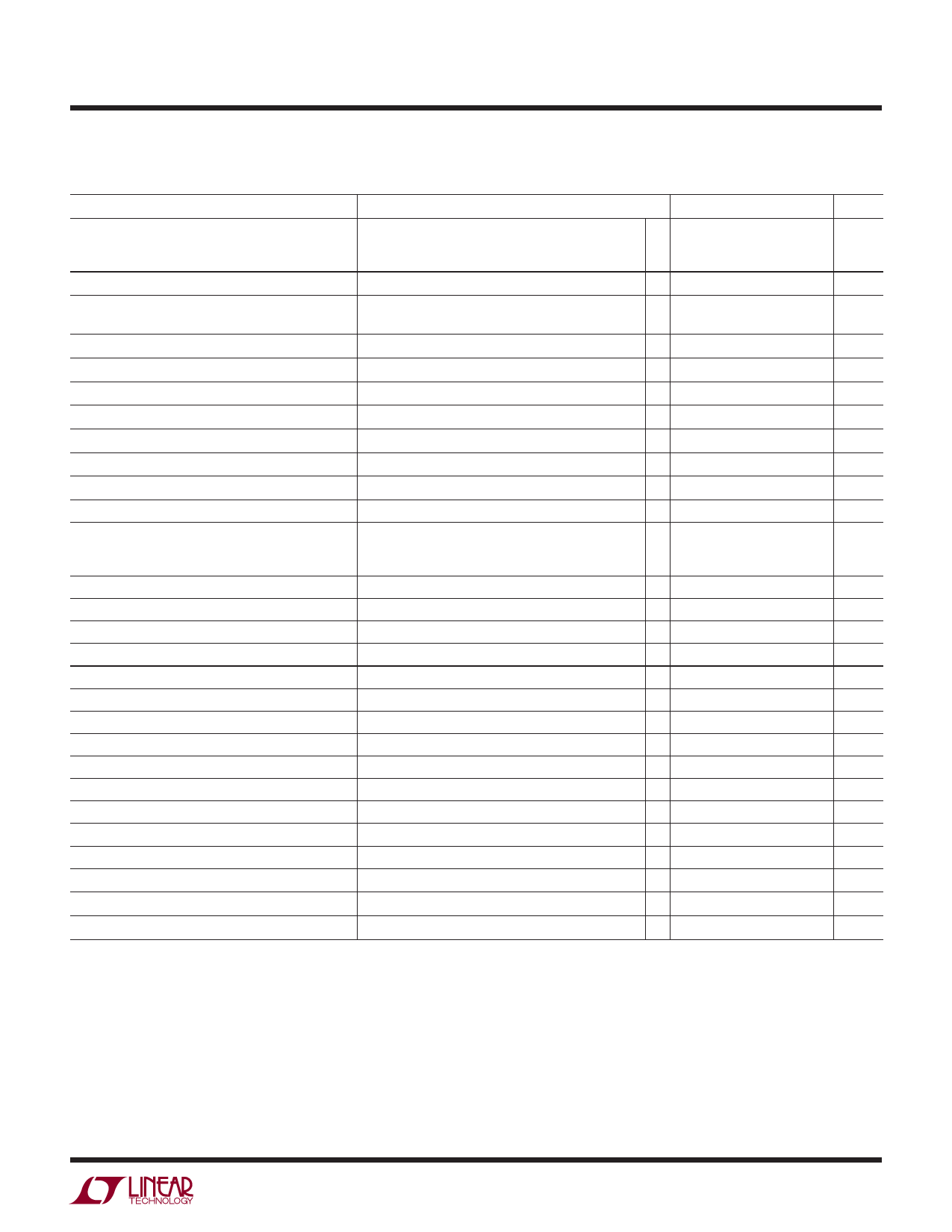
ELECTRICAL CHARACTERISTICS The ● denotes the specifications which apply over the full operating
temperature range, otherwise specifications are at TA = 25°C. VIN = 10V, VRUN/SS = 10V VBOOST = 15V, VBD = 3.3V unless otherwise
noted. (Note 2)
PARAMETER
Quiescent Current from BD
Minimum Bias Voltage (BD Pin)
Feedback Voltage
FB Pin Bias Current (Note 3)
FB Voltage Line Regulation
Error Amp gm
Error Amp Gain
CONDITIONS
VRUN/SS = 0.2V
VBD = 3V, Not Switching
VBD = 0, Not Switching
VC = 1.2V
4V < VIN < 36V
MIN
●
780
● 775
●
TYP MAX
0.01 0.5
0.9
1.3
1
5
2.7
3
790 800
790 805
7
30
0.002 0.01
500
1000
UNITS
μA
mA
μA
V
mV
mV
nA
%/V
μMho
VC Source Current
VC Sink Current
VC Pin to Switch Current Gain
VC Clamp Voltage
Switching Frequency
Minimum Switch Off-Time
Switch Current Limit
Switch VCESAT
Boost Schottky Reverse Leakage
Minimum Boost Voltage (Note 4)
BOOST Pin Current
RUN/SS Pin Current
RUN/SS Input Voltage High
RUN/SS Input Voltage Low
PG Threshold Offset from Feedback Voltage
PG Hysteresis
PG Leakage
PG Sink Current
SYNC Low Threshold
RT = 8.66k
RT = 29.4k
RT = 187k
Duty Cycle = 5%
ISW = 2A
VSW = 10V, VBD = 0V
ISW = 1A
VRUN/SS = 2.5V
VFB Rising
VPG = 5V
VPG = 0.4V
45
μA
45
μA
3.5
A/V
2
V
2.1
2.4
2.7
MHz
0.9
1
1.15
MHz
160
200
240
kHz
●
60
150
nS
3.2
3.7
4.2
A
500
mV
0.02
2
μA
●
1.5
2.1
V
22
35
mA
5
10
μA
2.5
V
0.2
V
90
mV
12
mV
0.1
1
μA
● 100
600
μA
0.5
V
SYNC High Threshold
0.7
V
SYNC Pin Bias Current
VSYNC = 0V
0.1
μA
Note 1: Stresses beyond those listed under Absolute Maximum Ratings
may cause permanent damage to the device. Exposure to any Absolute
Maximum Rating condition for extended periods may affect device
reliability and lifetime.
Note 2: The LT3685E is guaranteed to meet performance specifications
from 0°C to 125°C. Specifications over the –40°C to 125°C operating
temperature range are assured by design, characterization and correlation
with statistical process controls. The LT3685I specifications are
guaranteed over the –40°C to 125°C temperature range.
Note 3: Bias current flows out of the FB pin.
Note 4: This is the minimum voltage across the boost capacitor needed to
guarantee full saturation of the switch.
Note 5: Absolute Maximum Voltage at VIN and RUN/SS pins is 60V for
nonrepetitive 1 second transients, and 40V for continuous operation.
3685fb
3
Share Link: 